
Semiconductor storage device having a delayed sense amplifier activating signal during a test mode
Patent Information
- Authority / Receiving Office
- US · United States
- Current Assignee / Owner
- Publication Date
- 2001-07-10
- Estimated Expiration
- Not applicable · inactive patent
Smart Images
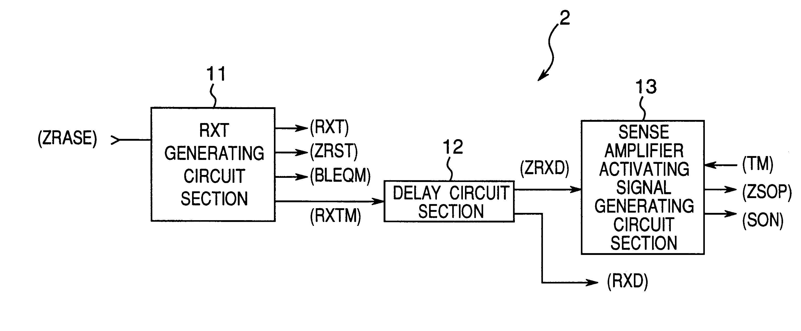
Figure 1 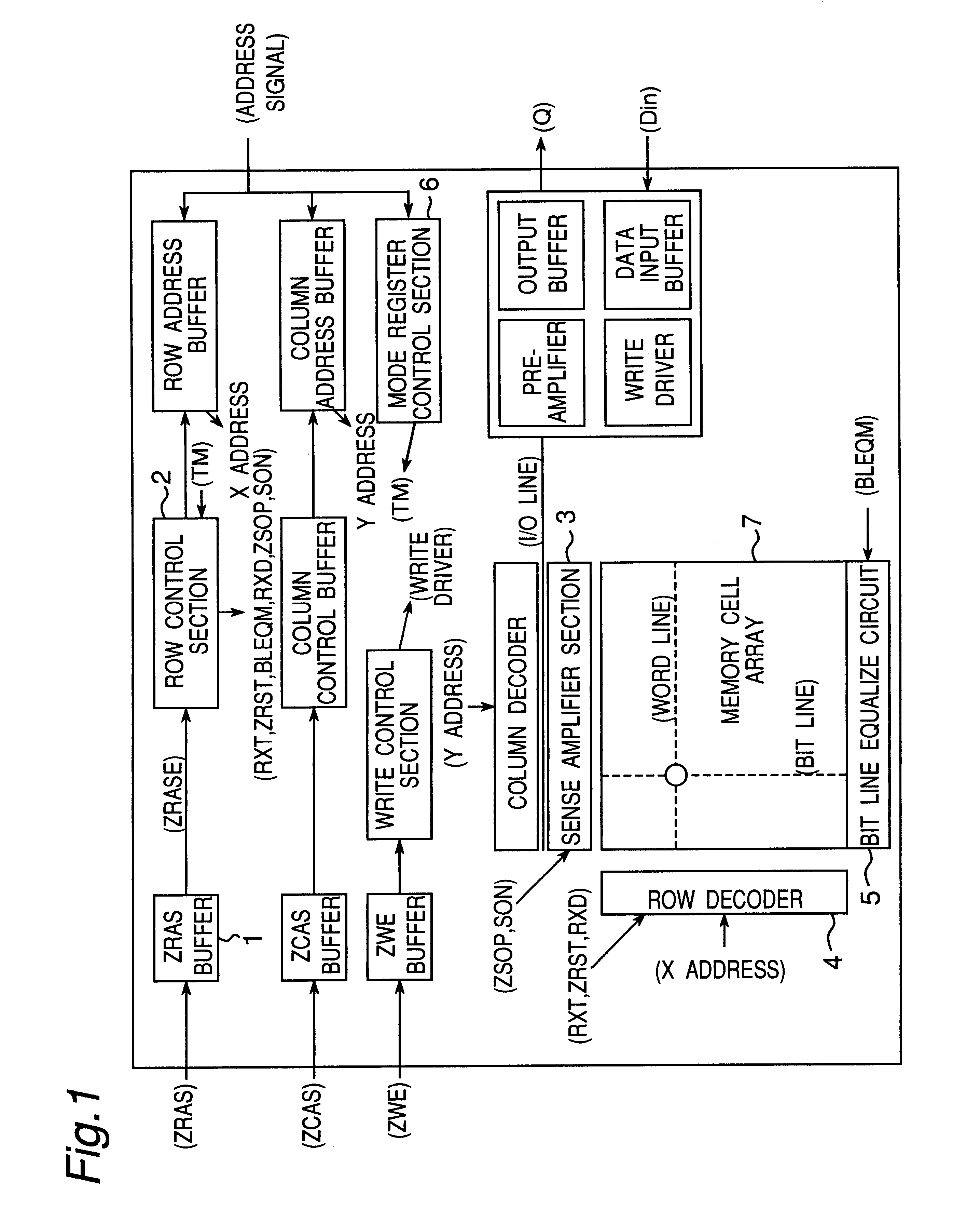
Figure 2 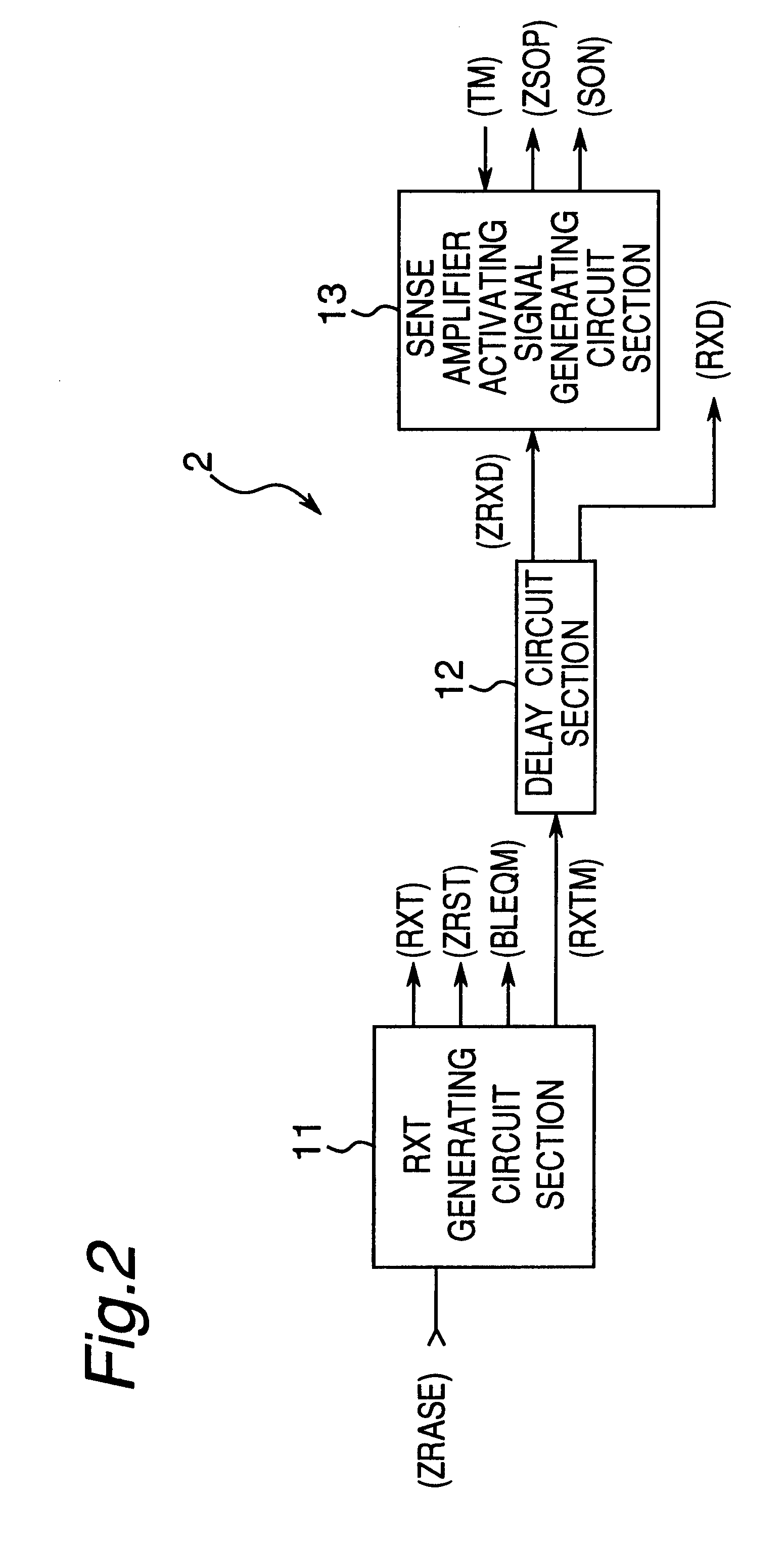
Figure 3
Abstract
Description
1. Field of the InventionThe present invention relates to a semiconductor storage device including a detecting circuit capable of detecting a shortcircuit between a storage node in a memory cell and a transistor gate, in particular, a high resistance shortcircuit therebetween.2. Description of the Related ArtIn a semiconductor storage device using a DRAM shown in FIG. 12, for example, when a voltage is applied to a gate TG of a transistor 101 in a memory cell 100, the transistor 101 is turned ON and electric charges stored in a capacity 102 are fed to a bit line BL through a storage node SN, accompanied by change of the electric potential of the bit line BL. A sense amplifier (not shown) serves to recognize the electric potential and to output the electric potential as magnitude data.In the process of manufacturing the memory cell for the semiconductor storage device, a shortcircuit has been caused between the gate TG of the transistor 101 constituting the memory cell 100 or between...
Examples
first embodiment
FIG. 1 is a schematic block diagram showing an example of a semiconductor storage device constituted by a DRAM. With reference to FIG. 1, description will be given to the operation of a ROW system related to the present invention, in particular, the activating signal of a sense amplifier, and the description of other operations will be omitted.
In FIG. 1, a ZRAS buffer 1 generates an internal RAS signal ZRASE from an externally input ROW address strobe signal (hereinafter referred to as an external RAS signal) ZRAS, and outputs the internal RAS signal ZRASE to a ROW control section 2.
The ROW control section 2 generates, from the input internal RAS signal ZRASE, a word line selection trigger signal RXT to be a trigger signal for selecting a word line, a reset signal ZRST, a bit line equalize signal BLEQM, a word line selection signal RXD, sense amplifier activating signals SON and ZSOP for activating each of the sense amplifiers of a sense amplifier section 3, and the like. The ROW co...
second embodiment
While the operation delay time of the sense amplifier in the test mode has a preset value in the first embodiment, the timing of the operation of the sense amplifier may be controlled in response to an externally input signal. In this respect, a second embodiment of the present invention will be described below in detail with reference to FIG. 11.
A sense amplifier activating signal generating circuit section 43 of a semiconductor storage device shown in FIG. 11 controls the rise of a generated sense amplifier activating signal SON and the fall of a sense amplifier activating signal ZSOP in response to an externally input write-enable signal ZWE in a test mode.
A schematic block diagram showing the semiconductor storage device according to the second embodiment of the present invention is the same as FIG. 1 except that the write-enable signal ZWE is externally input to a ROW control section, and a schematic block diagram showing an example of the structure of the ROW control section i...