
Confocal imaging
Patent Information
- Authority / Receiving Office
- US · United States
- Current Assignee / Owner
- Publication Date
- 2005-01-04
- Estimated Expiration
- Not applicable · inactive patent
Smart Images
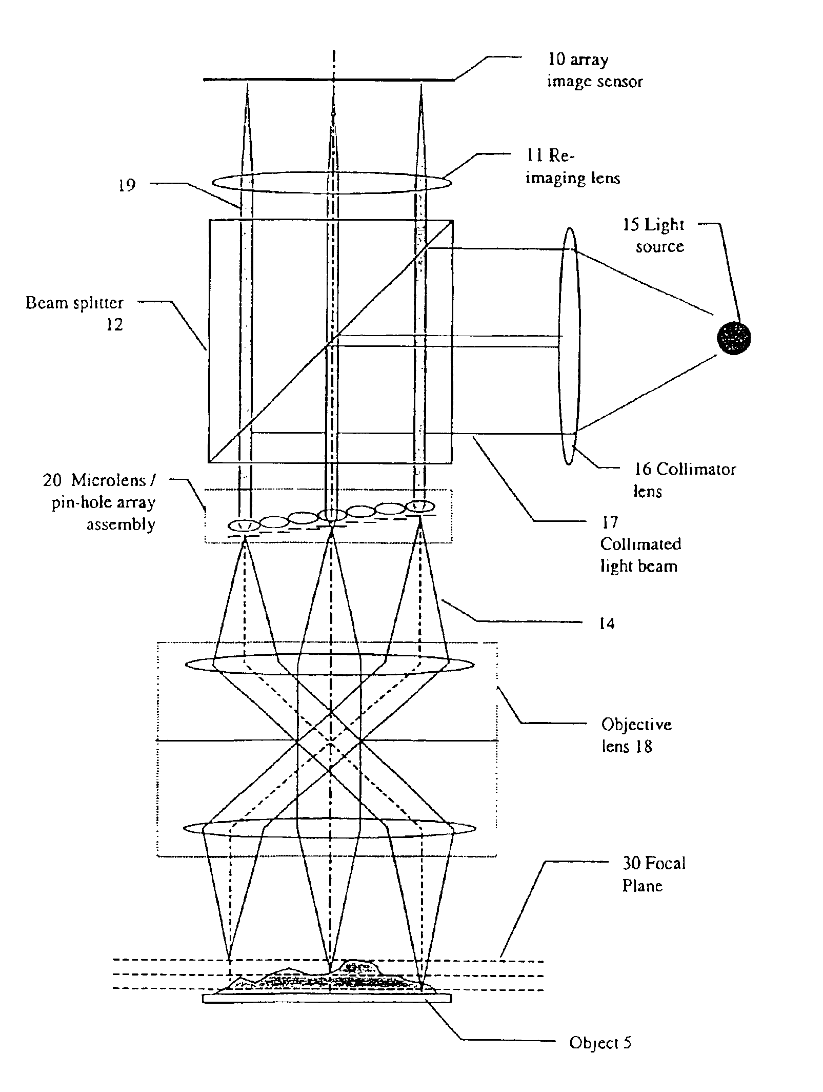
Figure 1 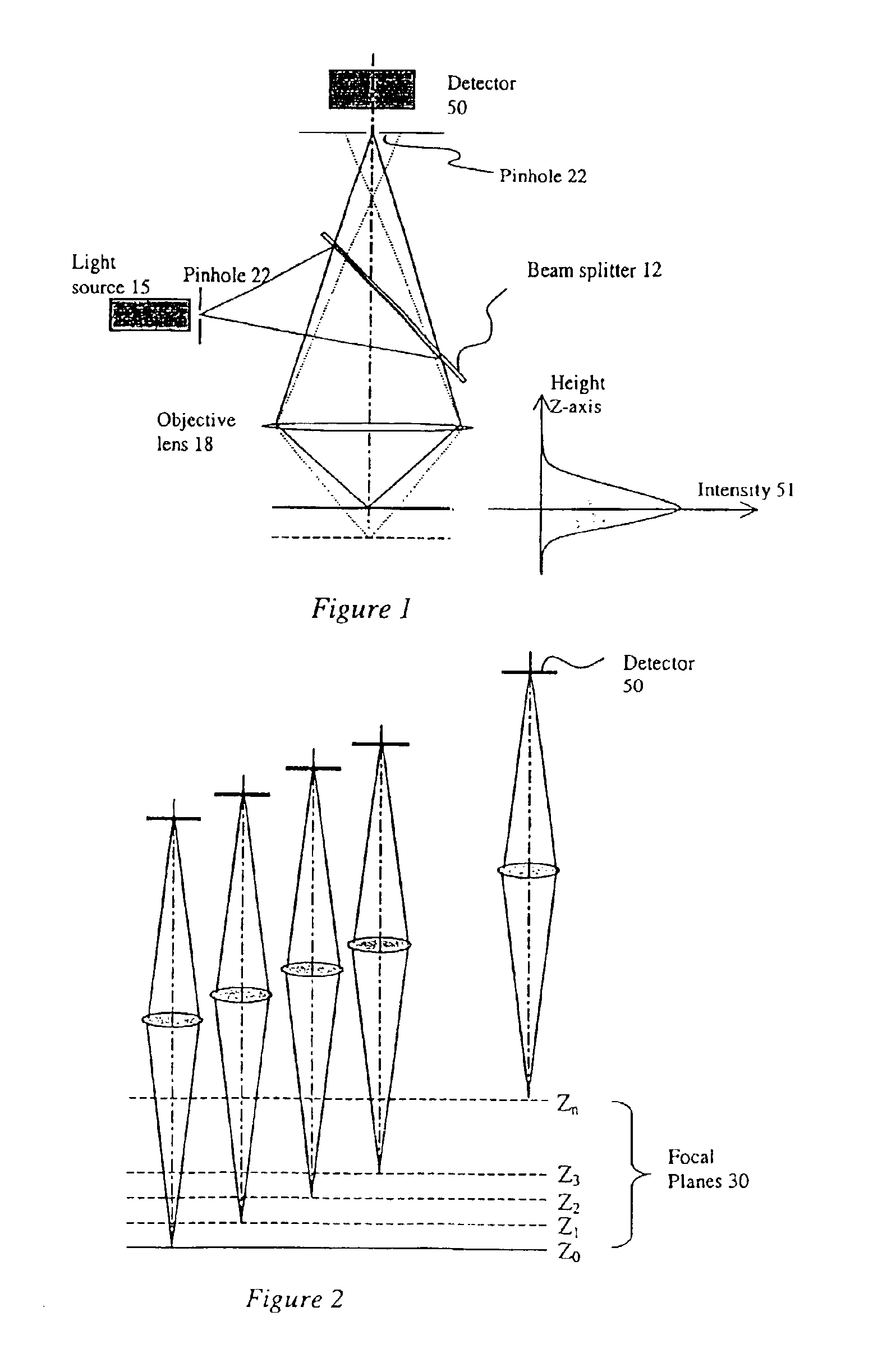
Figure 2 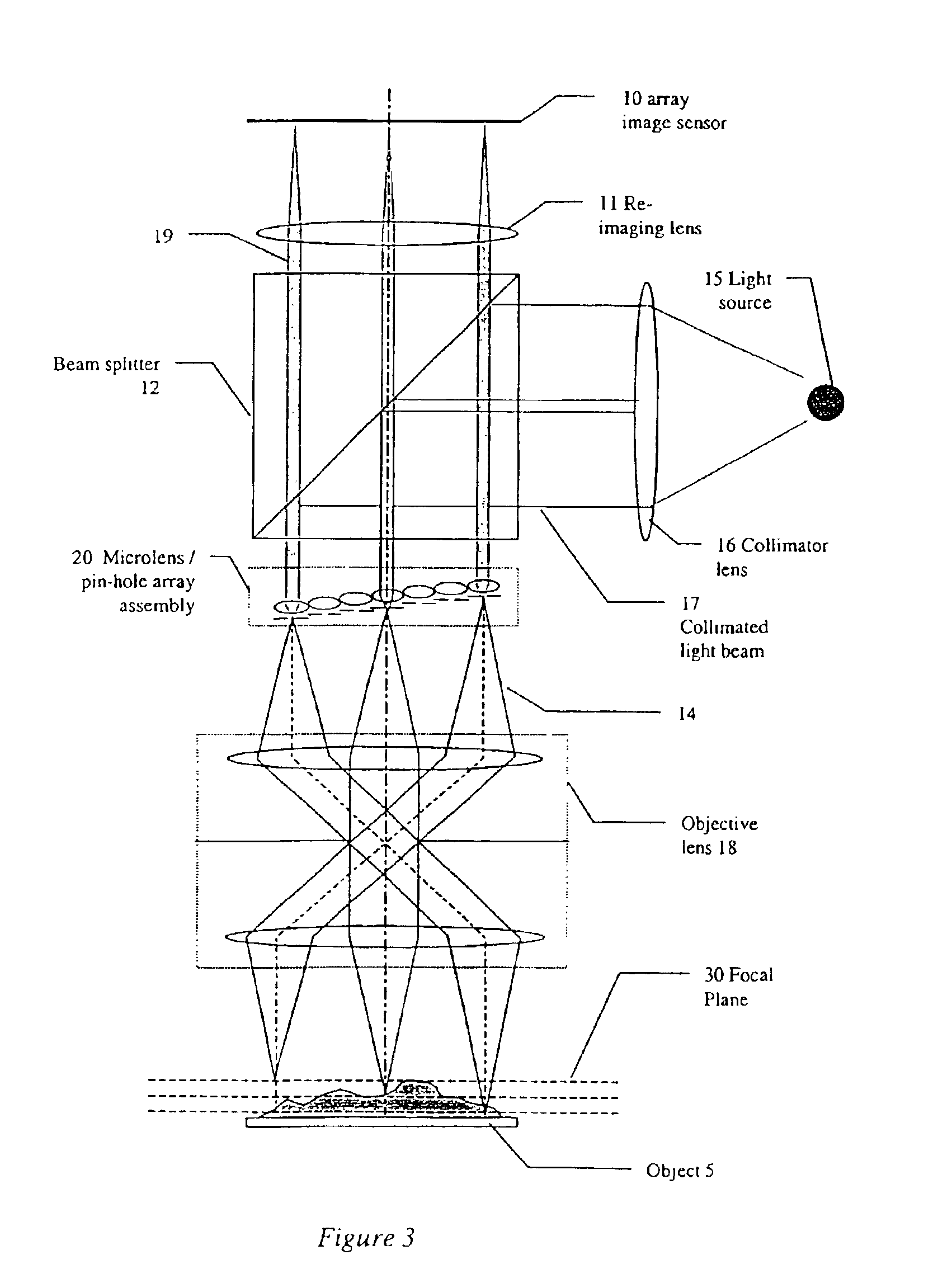
Figure 3
Abstract
Description
[0002] This invention relates to a system for high speed and high resolution confocal imaging for three dimensional measurement.BACKGROUND
[0003] The measurement of three dimensional features on a surface has many applications. One particular example is in the inspection of electronic components and electronic component assemblies.
[0004] The most common three dimensional inspection techniques available are optical techniques. These optical inspection techniques fall into several categories, including for example, structured light imaging, interferometry imaging, and triangulation imaging. There are drawbacks with each of these categories. One of the primary drawbacks is that the techniques are highly dependent on the reflective nature of the object under inspection. For example, when an object has specular surfaces, the triangulation imaging techniques which relies on true reflections will not work properly. Furthermore, when an object is surrounded by tall components, it may cause occl...
Examples
Embodiment Construction
view of a microlens and pinhole array for use in the confocal imaging system of FIG. 3.
[0029]FIG. 4(b) is a cross-sectional view A—A′ of the microlens and pinhole array of FIG. 4(a).
[0030]FIG. 5 shows an alternative design of the microlens and pinhole array for use in the confocal imaging system of FIG. 3.
[0031]FIG. 6 is an illustration showing the relationship between the image and the object space.
[0032]FIG. 7 shows a block diagram of the image sensor, processing and control modules in accordance with the present invention.
[0033]FIG. 8 is a flow chart showing the major steps of computing the 3D map of an object.
DESCRIPTION OF A SPECIFIC EMBODIMENT
[0035]Referring to FIG. 3, there is shown a confocal imaging system for inspecting an object 5 to determine the three dimensional surface structure of the object. The confocal imaging system comprises a light source 15, and a collimator lens 16 for refracting light from the light source into a collimated light...