
Trench capacitor of a DRAM and fabricating method thereof
a technology of dram and clamp capacitor, which is applied in the direction of semiconductor devices, electrical devices, transistors, etc., can solve the problems of increasing the number of technical problems encountered in the fabrication of both types of dram, limiting and increasing the amount of memory needed to operate software at an alarming rate. , to achieve the effect of increasing the level of device integration and a larger processing window
Patent Information
- Authority / Receiving Office
- US · United States
- Patent Type
- Patents(United States)
- Current Assignee / Owner
- Publication Date
- 2008-08-05
Smart Images
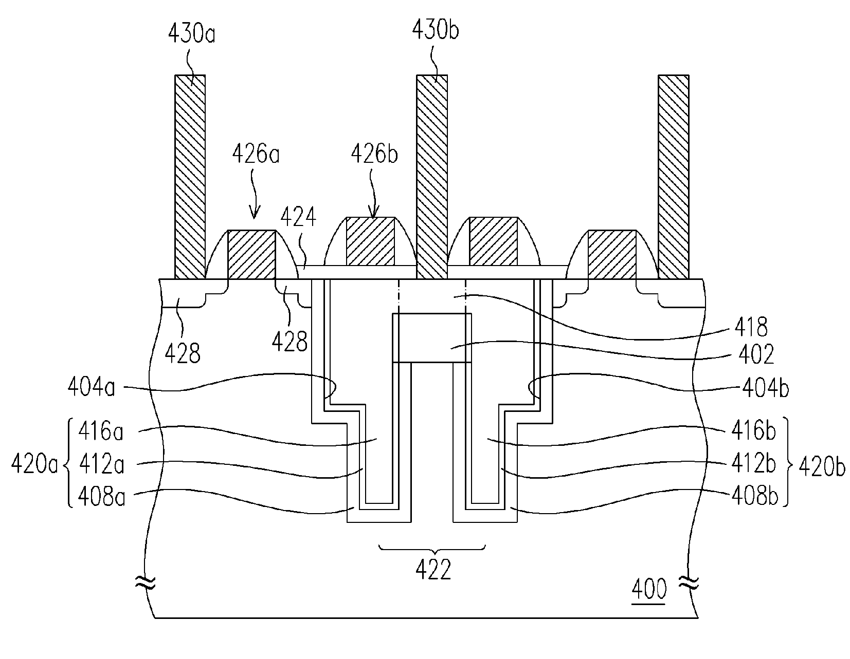
Figure 1 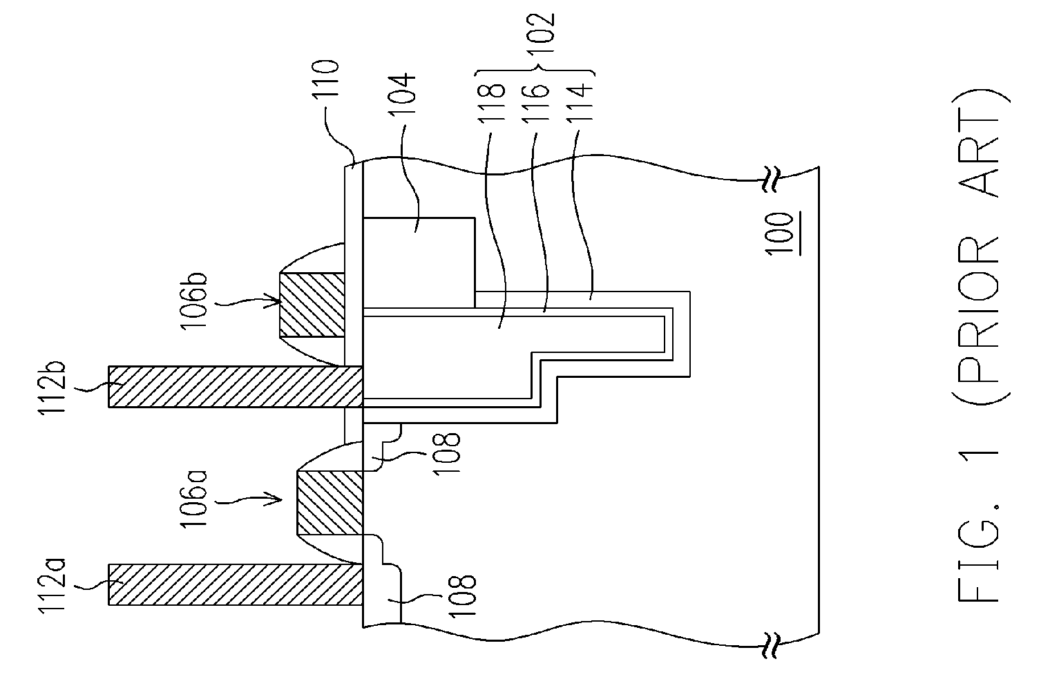
Figure 2 
Figure 3
Abstract
Description
BACKGROUND OF THE INVENTION
[0001] 1. Field of the Invention
[0002] The present invention relates to a dynamic random access memory (DRAM). More particularly, the present invention relates to a trench capacitor of a DRAM and fabricating method thereof.
[0003] 2. Description of the Related Art
[0004] As semiconductor finally enters the deep sub-micron regime, the dimensions of each device are significantly reduced. This means that the area for accommodating the capacitors of a DRAM is correspondingly reduced. On the other hand, with the ever-increasing size of computer application software, the amount of memory needed to operate the software also increases at an alarming rate. Such conflicting demand for a smaller dimension and a larger memory storage capacity implies that the former method of fabricating the capacitors of a DRAM must be modified to fit this trend.
[0005] According to the structure of capacitor, the DRAM can be classified into two major types, namely, the stack capacitor DRAM ...
Examples
first embodiment
[0036]FIGS. 4A through 4E are schematic cross-sectional views showing the steps for fabricating a DRAM according to one preferred embodiment of the present invention. First, as shown in FIG. 4A, a substrate 300 is provided. The substrate has at least an isolation structure 302 formed thereon. The substrate 300 is a silicon substrate and the isolation structure 302 is a shallow trench isolation (STI) structure fabricated using silicon oxide, for example.
[0037]Then, trenches 304a and 304b are formed in the substrate 300 beside the isolation structure 302. The trenches 304a and 304b are formed, for example, by performing a patterning process using a mask layer. In one embodiment, the trenches 304a and 304b penetrate through the isolation structure 302. The dash line portion represents that portion of the isolation structure 302 is removed in the process of forming the trenches 304a and 304b.
[0038]After that, a first lower electrode 306a and a second lower electrode 306b are formed in ...
second embodiment
[0048]FIGS. 5A through 5E are schematic cross-sectional views showing the steps for fabricating a DRAM according to another preferred embodiment of the present invention. First, as shown in FIG. 5A, a substrate 400 is provided. The substrate has at least an isolation structure 402 formed thereon. The substrate 400 is a silicon substrate and the isolation structure 402 is a shallow trench isolation (STI) structure fabricated using silicon oxide, for example.
[0049]Trenches 404a and 404b are formed in the substrate 400 beside the isolation structure 402 and then a portion of the isolation structure 402 between the trenches 404a and 404b is removed to form an opening 406. The trenches 404a and 404b and the opening 406 are formed, for example, by performing a patterning process using a mask layer. In one embodiment, the trenches 404a and 404b penetrate through the isolation structure 402. The dash line portion represents that portion of the isolation structure 402 is removed in the proce...