
High voltage semiconductor device and method of manufacture thereof
a semiconductor and high-voltage technology, applied in the direction of semiconductor devices, basic electric elements, electrical apparatus, etc., can solve the problem of insufficient breakdown voltage in this portion, and achieve the effect of suppressing the lowering of breakdown voltage, reducing current crowding, and reducing current density
Patent Information
- Authority / Receiving Office
- US · United States
- Patent Type
- Patents(United States)
- Current Assignee / Owner
- Publication Date
- 2009-10-13
- Estimated Expiration
- Not applicable · inactive patent
Smart Images
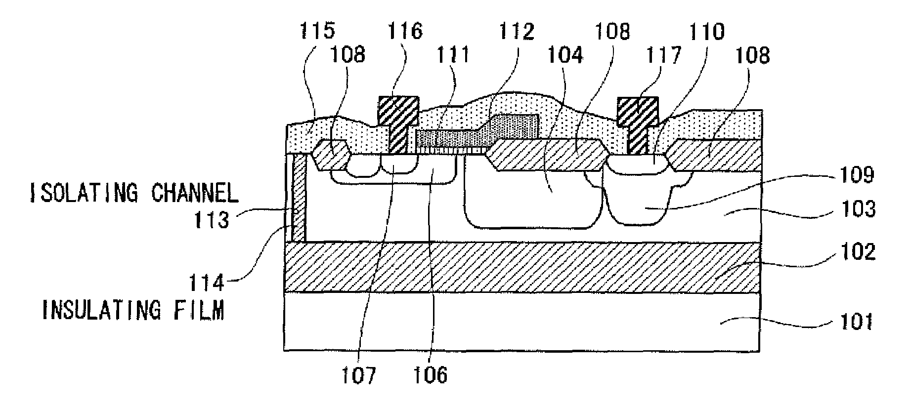
Figure 1 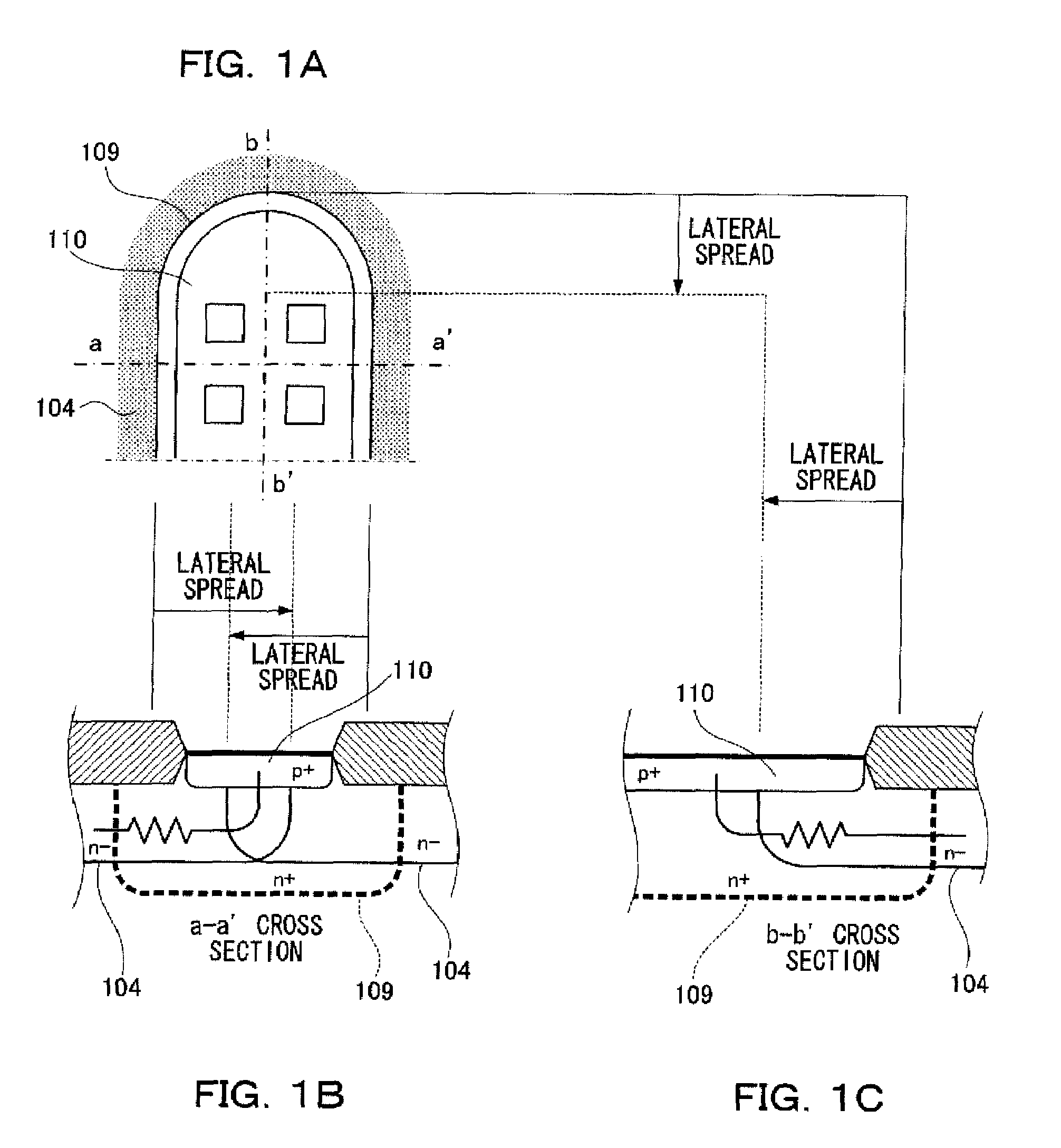
Figure 2 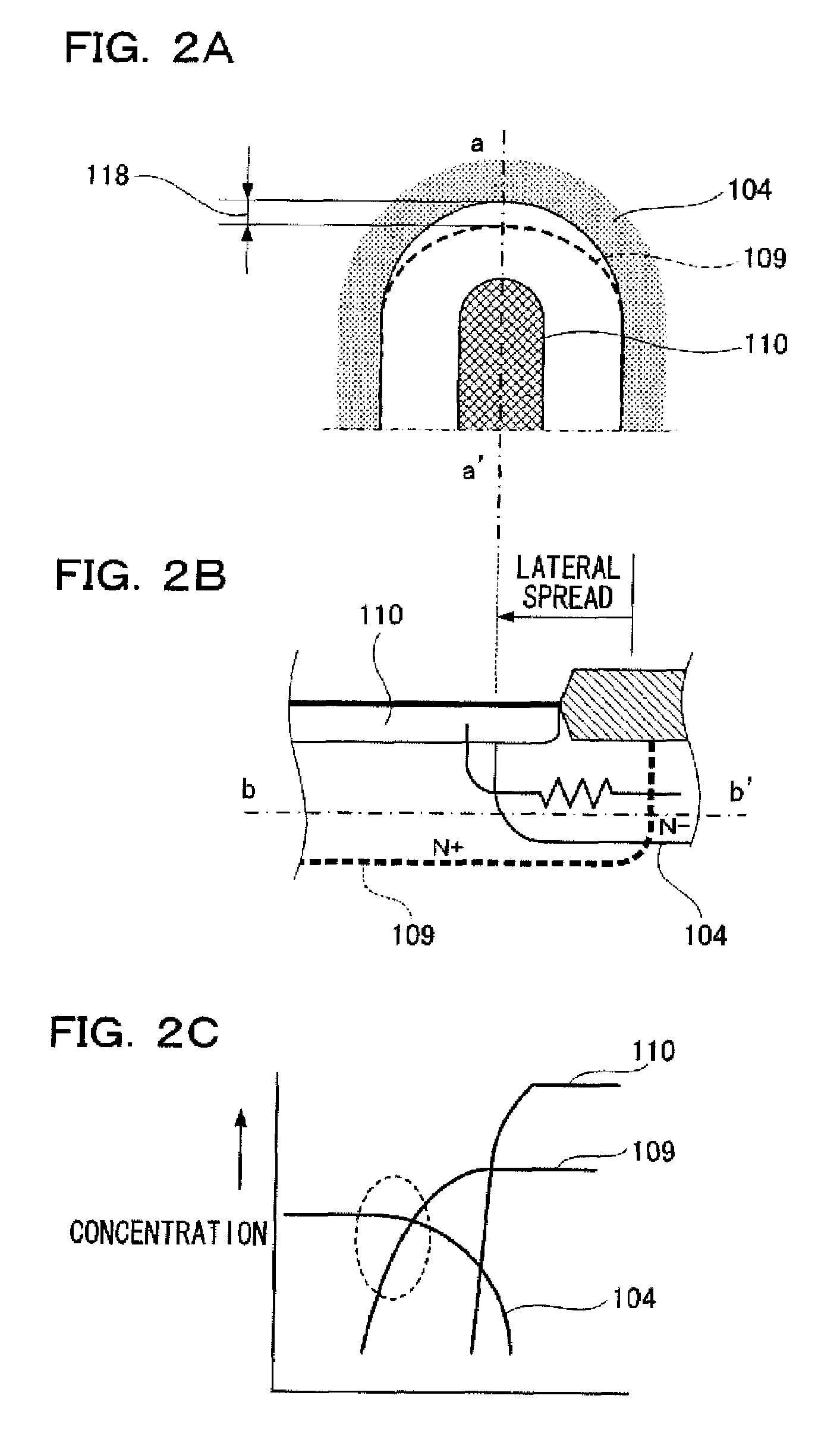
Figure 3
Abstract
Description
FIELD OF THE INVENTION
[0001] The present invention relates to a high voltage semiconductor device and a method of manufacture thereof, and more specifically to an insulated gate bipolar transistor (hereafter abbreviated as “IGBT”) that realizes high breakdown voltage while maintaining a short turnoff time and a low on-voltage.BACKGROUND OF THE INVENTION
[0002] For isolating elements in a semiconductor device, a large number of junction isolating techniques using p-n junction have been used for a long time. In recent years, however, dielectric isolation wherein in an SOI (silicon on insulator) substrate having a buried insulating film, a trench that extends from the surface of the substrate to the buried insulating film is formed, and an insulating film is formed in the trench, has been used.
[0003] Such an element structure of SOI-trench isolation is especially effective in semiconductor devices for high breakdown voltage power fields wherein the formation of deep isolation is generally ...
Examples
first embodiment
[0045]An IGBT, which is a high voltage semiconductor device according to a first embodiment of the present invention, will be described referring to the drawings.
[0046]FIG. 1A is a plan structural diagram illustrating that an n+-type collector buffer layer 109 is formed on a p-type silicon layer 103 adjacent to an n−-type drift diffusion layer 104 in the IGBT of the present invention. FIGS. 1B and 1C are cross-sectional structural diagrams along the line a-a′ and the line b-b′ in FIG. 1A, respectively.
[0047]The present invention differs from the conventional examples in that in the conventional examples, an n-type drift diffusion layer 104 is formed so as to completely include the region of an n+-type collector buffer layer 109, whereas in the IGBT of the present invention shown in FIGS. 1A to 1C, an n−-type drift diffusion layer 104 is formed so as to surround the n+-type collector buffer layer 109. Since other structures are basically identical to those in the conventional example...
second embodiment
[0052]Next, an IGBT, which is a high voltage semiconductor device according to a second embodiment of the present invention, will be described referring to the drawings.
[0053]FIG. 2A is a plan structural diagram of an IGBT, which is the high voltage semiconductor device according to the second embodiment of the present invention; FIG. 2B is a cross-sectional structural diagram along the line a-a′ in FIG. 2A; and FIG. 2C is a graph showing an impurity concentration profile of the n+-type collector buffer layer 109 and the n−-type drift diffusion layer 104 in the vicinity of the line b-b′ in FIG. 2B.
[0054]The IGBT in the second embodiment has a structure and components identical to those of the IGBT in the first embodiment shown in FIGS. 1A and 1B except the location of the n−-type drift diffusion layer 104 relative to the p+-type collector diffusion layer 110 and the n+-type collector buffer layer 109. Therefore, the description for the same components will be omitted by using the sa...
third embodiment
[0058]Next, an IGBT, which is a high voltage semiconductor device according to a third embodiment of the present invention, will be described referring to the drawings.
[0059]FIG. 3A is a plan structural diagram of the IGBT, which is the high voltage semiconductor device according to the third embodiment of the present invention; FIG. 3B is a cross-sectional structural diagram along the line a-a′ in FIG. 3A; and FIG. 3C is a graph showing an impurity concentration profile of the n+-type collector buffer layer 109 and the n−-type drift diffusion layer 104 in the vicinity of the line b-b′ in FIG. 3B.
[0060]The IGBT in the third embodiment has a structure and components identical to those of IGBTs in the first and second embodiments shown in FIGS. 1 and 2 except the location of the n+-type collector buffer layer 109 relative to the p+-type collector diffusion layer 110. Therefore, the description for the same components will be omitted by using the same reference numerals and characters ...