
Nanowire multispectral imaging array
a multi-spectral imaging and array technology, applied in the field of infrared detectors and imaging arrays, can solve the problems of high vacuum, inability to meet the sensitivity of individual microbolometer pixels, and inability to respond uniformly to infrared radiation, so as to increase the manufacturability of multi-spectral imaging array systems and reduce thermal time constants , the effect of high frame ra
Patent Information
- Authority / Receiving Office
- US · United States
- Patent Type
- Patents(United States)
- Current Assignee / Owner
- Publication Date
- 2010-08-31
Smart Images
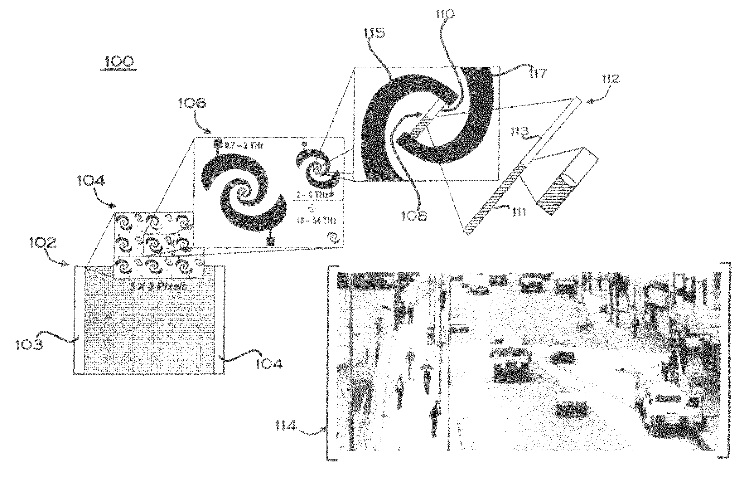
Figure 1 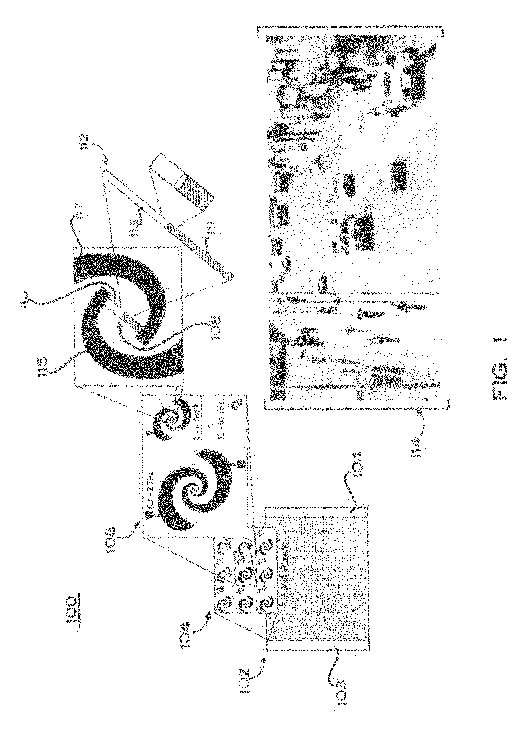
Figure 2 
Figure 3
Abstract
Description
CROSS-REFERENCE TO PROVISIONAL PATENT APPLICATION
[0001] This application claims the benefit of U.S. Provisional Patent application Ser. No. 60 / 972,120, entitled “Nanowire Multispectral Imaging Array”, which was filed on Sep. 13, 2007.TECHNICAL FIELD
[0002] Embodiments are generally related to imaging arrays and infrared detectors. Embodiments are also related to microbolometers and imaging systems that employ microbolometer components. Embodiments are also related to nanowires and nanotechnology-based components.BACKGROUND OF THE INVENTION
[0003] Infrared (IR) detectors are often utilized to detect fires, overheating machinery, planes, vehicles, people, and any other objects that emit thermal radiation. Infrared detectors are unaffected by ambient light conditions or particulate matter in the air such as smoke or fog. Thus, infrared detectors have potential use in night vision and when poor vision conditions exist, such as when normal vision is obscured by smoke or fog. IR detectors are ...
Examples
Embodiment Construction
[0021]The particular values and configurations discussed in these non-limiting examples can be varied and are cited merely to illustrate at least one embodiment of the present invention and are not intended to limit the scope of the invention.
[0022]The embodiments disclosed herein describe how to obtain a high frame rate for a high pixel count by utilizing nanowires as the microbolometer sensing element. The nanowire(s) allows for using antennas printed on the same dielectric substrate with a size covering a range of 0.8-54 THz because it effectively replaces the microbridge and can be scaled in length to match the gap between the antennas. Moreover the very small diameter of the nanowire decreases the thermal time constant and therefore increases the read-out rate.
[0023]At the same time, the nanowire small diameter decreases the ambient gas cooling speed relative to the read-out rate in the package which makes the vacuum package more manufacturable. The material properties of the n...