
Linearity improvements of semiconductor substrate using passivation
a technology of semiconductor substrates and passivation, applied in the direction of semiconductor devices, diodes, electrical apparatus, etc., can solve the problems of non-linear capacitance, non-linear conductance, non-linear capacitance, affecting the rf interaction between the silicon substrate and other layers, and achieving the effect of effectively immobilizing the surface conduction layer, preventing capacitance and inductance changes, and high density of traps
Patent Information
- Authority / Receiving Office
- US · United States
- Current Assignee / Owner
- Publication Date
- 2011-03-29
Smart Images
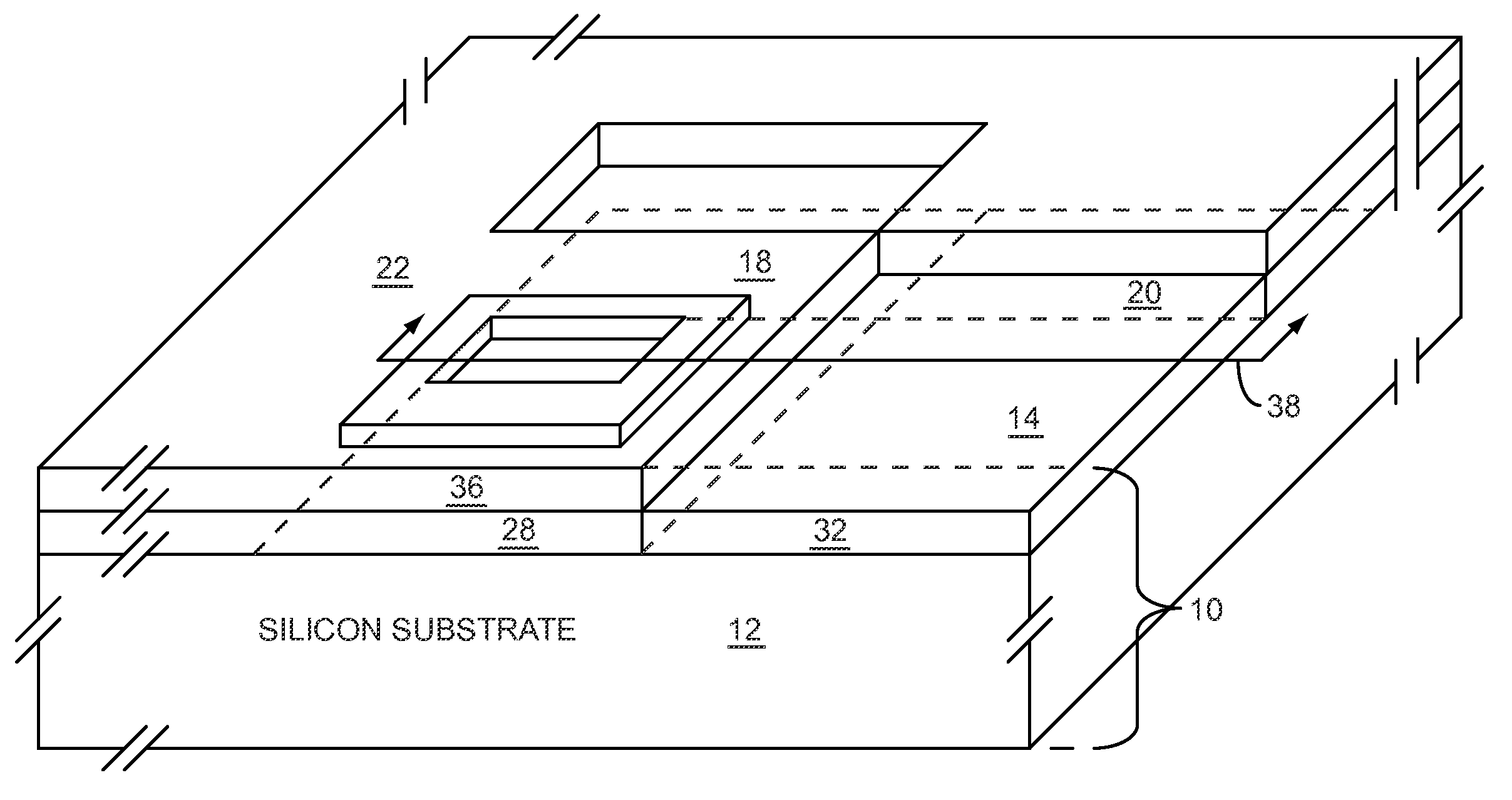
Figure 1 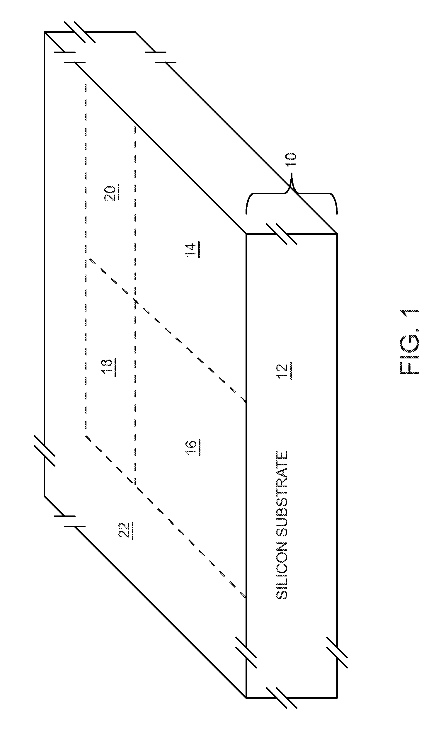
Figure 2 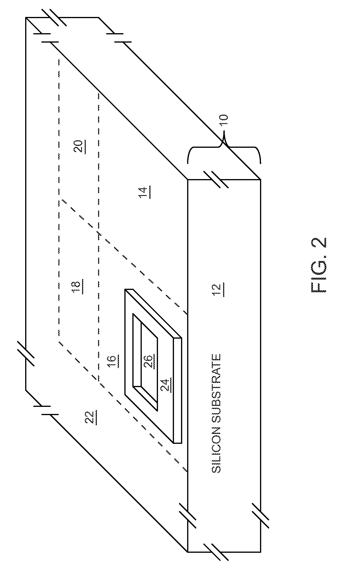
Figure 3
Abstract
Description
[0001] This application claims the benefit of provisional patent application Ser. No. 60 / 948,597 filed Jul. 9, 2007, the disclosure of which is hereby incorporated herein by reference in its entirety.FIELD OF THE INVENTION
[0002] Embodiments of the present invention relate to semiconductor substrates used to manufacture semiconductor devices, which may be used in radio frequency (RF) communications systems.BACKGROUND OF THE INVENTION
[0003] Silicon substrates are widely used in the manufacture of semiconductor devices. Low cost and highly evolved manufacturing techniques make Silicon a preferred material in many applications, when compared with other semiconductor materials. Standard complementary metal oxide semiconductor (CMOS) process techniques are often used with Silicon and are highly evolved and cost effective. High resistivity Silicon substrates may be used in radio frequency (RF) devices. If the period of an RF signal is shorter than a majority carrier relaxation time, then the ...
Examples
Embodiment Construction
[0006]The present invention relates to using a potentially trap-rich layer, such as a polycrystalline Silicon layer, over a passivation region of a semiconductor substrate or a Silicon-on-insulator (SOI) device layer to substantially immobilize a surface conduction layer at the surface of the semiconductor substrate or SOI device layer at radio frequency (RF) frequencies. The potentially trap-rich layer may have a high density of traps that trap carriers from the surface conduction layer. The average release time from the traps may be longer than the period of any present RF signals, thereby effectively immobilizing the surface conduction layer, which may substantially prevent capacitance and inductance changes due to the RF signals. Therefore, harmonic distortion of the RF signals may be significantly reduced or eliminated. The semiconductor substrate may be a Silicon substrate, a Gallium Arsenide substrate, or another substrate.
[0007]The semiconductor substrate or SOI device layer...