

Semiconductor memory cell and manufacturing method thereof, and semiconductor memory devices
Patent Information
- Authority / Receiving Office
- US · United States
- Current Assignee / Owner
- Publication Date
- 2013-02-26
- Estimated Expiration
- Not applicable · inactive patent
Smart Images
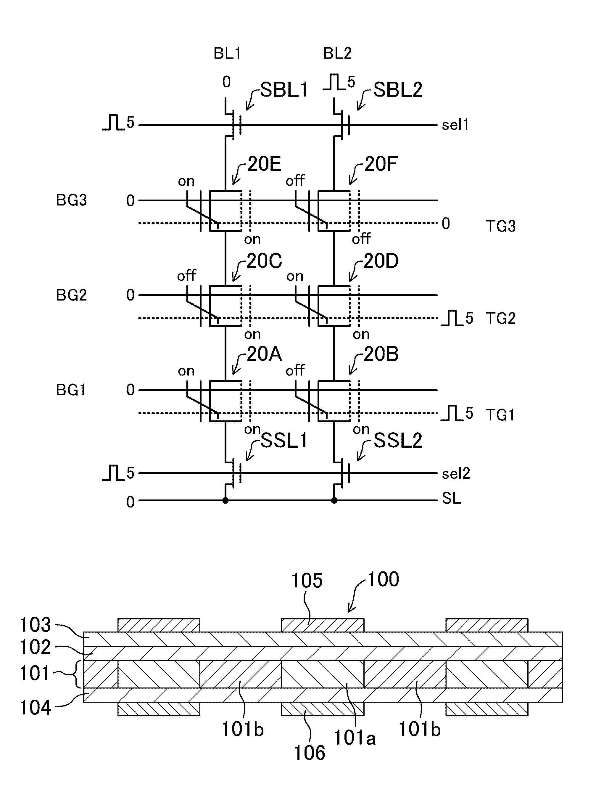
Figure 1 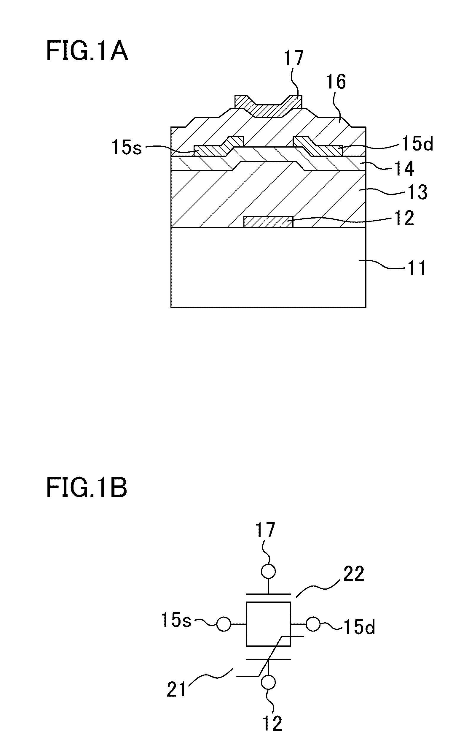
Figure 2 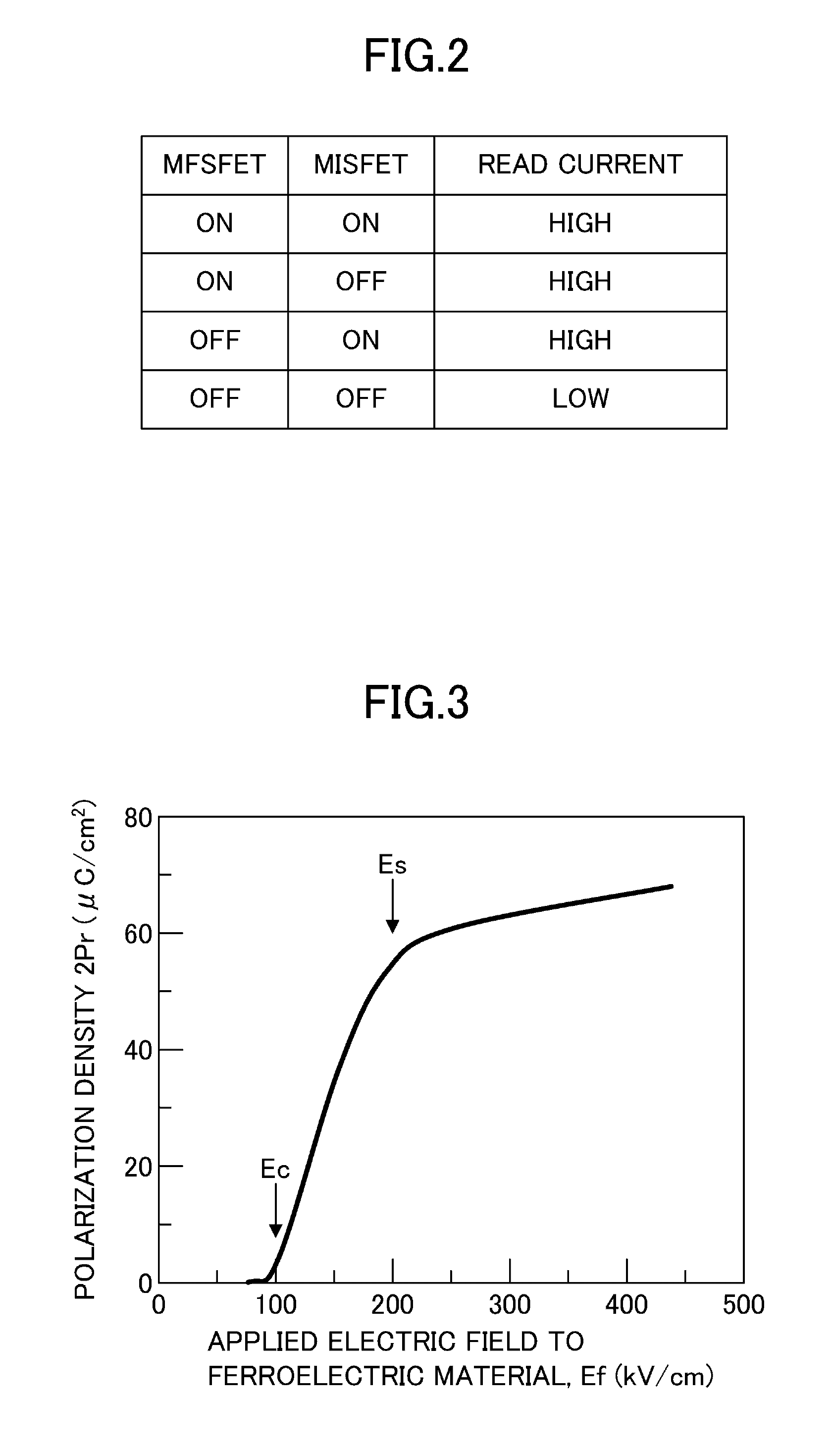
Figure 3
Abstract
Description
CROSS-REFERENCE TO RELATED APPLICATION
[0001] This is a continuation of PCT International Application PCT / JP2009 / 005595 filed on Oct. 23, 2009, which claims priority to Japanese Patent Application No. 2009-040878 filed on Feb. 24, 2009, Japanese Patent Application No. 2009-054919 filed on Mar. 9, 2009, and Japanese Patent Application No. 2009-119619 filed on May 18, 2009. The disclosures of these applications including the specifications, the drawings, and the claims are hereby incorporated by reference in their entirety.BACKGROUND
[0002] The present invention relates to semiconductor memory cells including a memory element formed by a field effect transistor having a gate insulating film made of a ferroelectric film, and semiconductor memory devices having semiconductor memory cells arranged in an array.
[0003] Nonvolatile memories using a ferroelectric material are roughly divided into two types, namely a capacitor type and a field effect transistor (FET) type having a gate insulating f...
Examples
first embodiment
[0048](First Embodiment)
[0049]FIGS. 1A-1B are diagrams schematically showing a configuration of a semiconductor memory cell in a first embodiment of the present invention, where FIG. 1A is a cross-sectional view of the semiconductor memory cell, and FIG. 1B is an equivalent circuit diagram thereof.
[0050]As shown in FIG. 1A, a ferroelectric film 13 and a paraelectric film 16 are stacked together over a substrate 11 with a semiconductor film 14 interposed between the ferroelectric film 13 and the paraelectric film 16. A first gate electrode 12 of a first field effect transistor (FET) is formed on the side of the ferroelectric film 13, and a second gate electrode 17 of a second FET is formed on the side of the paraelectric film 16 so as to face the first gate electrode 12. The semiconductor film 14 is made of a compound semiconductor that forms a common channel layer of the first and second FETs, and a common source electrode 15s and a common drain electrode 15d of the first and second...
second embodiment
[0090](Second Embodiment)
[0091]In the NAND-type nonvolatile memory described in Patent Document 2, data written to a selected memory cell is read by turning off only the MISFET of this memory cell and turning on the other MISFETs, and measuring a current flowing in a memory block where the memory cells are connected in series.
[0092]Since FETs having a gate insulating film of a paraelectric material are used as the MISFETs of these memory cells, these MISFETs are also used for select transistors of the memory block. Thus, these MISFETs are usually of a normally-off type. When reading the nonvolatile memory using the normally-off type transistors, a voltage is applied to the gate electrodes in order to turn on the MISFETs of the non-selected memory cells. As a result, the polarization state of the ferroelectric film of the non-selected memory cells is reversed, which may disturb the data written in the memory cell.
[0093]When reading the nonvolatile memory, a predetermined voltage need...
third embodiment
[0119](Third Embodiment)
[0120]The semiconductor memory device that does not cause disturbance in read operation of the semiconductor memory cells is described in the second embodiment. A semiconductor memory device that does not cause disturbance in write operation to semiconductor memory cells will be described in a third embodiment of the present invention.
[0121]Write operation to the semiconductor memory cells (hereinafter simply referred to as the “memory cells”) arranged in an array will be described with reference to FIGS. 19A-22B. An example will be described in which memory cells 20A-20F are arranged in three rows by two columns. MISFETs forming select switching elements of the memory cells are of a normally-on type.
[0122]First, reset operation that is performed before write operation will be described with reference to FIGS. 19A-19B. FIG. 19A is a circuit diagram showing a memory cell layout, and FIG. 19B is a timing chart of the reset operation.
[0123]As shown in FIG. 19A, ...