
Electroplating wafers having a notch
a technology of electroplating wafers and notch edges, which is applied in the direction of electrolysis components, electrolysis processes, contact devices, etc., can solve the problems of non-uniform plating, reducing the yield of the wafer, and increasing the time requirements and complexity of the manufacturing process, so as to reduce the current crowding effect, thin plating, and uniform thickness
Patent Information
- Authority / Receiving Office
- US · United States
- Patent Type
- Patents(United States)
- Current Assignee / Owner
- Publication Date
- 2017-06-27
Smart Images
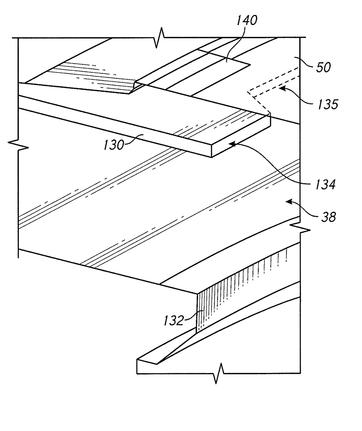
Figure 1 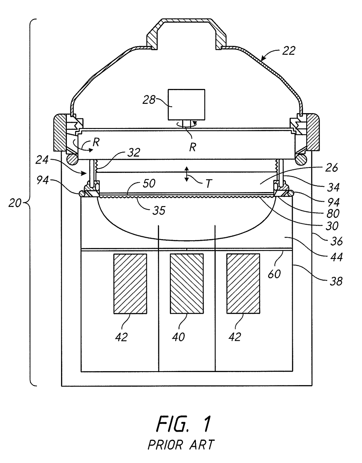
Figure 2 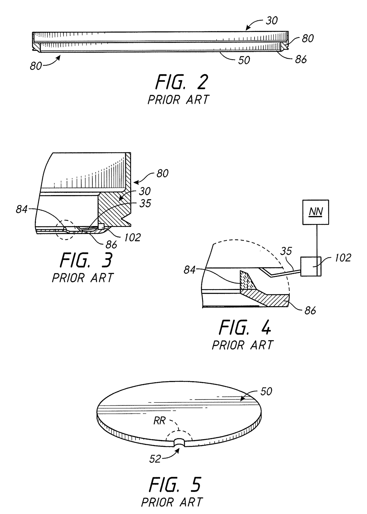
Figure 3
Abstract
Description
BACKGROUND OF THE INVENTION
[0001] Manufacture of semiconductor integrated circuits and other micro-scale devices typically requires formation of multiple metal layers on a wafer or other substrate. By electroplating metals layers in combination with other steps, such as planarizing, etching and photolithography, patterned metal layers forming the micro-scale devices are created.
[0002] Electroplating is performed with the wafer, or one side of the substrate, in a bath of liquid electrolyte, and with electrical contacts on a contact ring touching a conductive layer on the wafer surface. Electrical current is passed through the electrolyte and the conductive layer. Metal ions in the electrolyte deposit or plate out onto the wafer, creating a metal film on the wafer. The metal ions also tend to plate out onto the electrical contacts as well, which changes the electric field around the contacts, causing non-uniform plating. The metal plated onto the electrical contacts consequently must be...
Examples
Embodiment Construction
[0022]To achieve a high yield of devices from each wafer, the edge zone which is contacted by the seal must be as small as possible. In the past, an edge zone of 2 or 3 mm (i.e., the annular ring at the wafer edge not useable for manufacturing devices) was often acceptable. With current industry requirements, the edge zone is now approaching or already at 1 mm. Referring momentarily to FIG. 5, some wafers 50 have a notch 52 (enlarged for illustration). On a 300 mm diameter wafer 50, the notch 52 extends in 1.5 mm. Therefore, the seal used for processing these types of wafers has an inward projection at the notch to avoid plating fluid leaking through the notch. The resulting seal covers more of the wafer around the notch. This changes the electric field in the region around the notch, causing the plated film around the notch to be thicker than the plated film on the rest of the wafer, due to current crowding at the notch.
[0023]One method to improve uniformity near the notch is to re...