Achieving High-Resolution Displays with QNED
JUN 19, 20258 MIN READ
Generate Your Research Report Instantly with AI Agent
Patsnap Eureka helps you evaluate technical feasibility & market potential.
QNED Display Evolution
QNED (Quantum Nano-Emitting Diode) display technology has undergone significant evolution since its inception, marking key milestones in the pursuit of high-resolution displays. The journey began with the conceptualization of quantum dot technology in the early 2000s, which laid the foundation for QNED development.
In the initial phase, researchers focused on enhancing the color gamut and brightness of displays using quantum dots. This led to the introduction of quantum dot-enhanced LCD screens, which offered improved color accuracy and vibrancy compared to traditional LCD displays. However, these early implementations still relied on LED backlighting, limiting their potential for true blacks and high contrast ratios.
The next significant leap came with the development of self-emissive quantum dot displays. This breakthrough allowed each pixel to emit its own light, eliminating the need for a separate backlight. This advancement paved the way for QNED technology, which combines the color purity of quantum dots with the self-emissive properties of nano-scale LEDs.
QNED displays entered the research and development phase in the mid-2010s, with major electronics manufacturers investing heavily in this promising technology. The primary focus was on overcoming challenges related to manufacturing processes, stability, and scalability of quantum dot-based emitters.
By the late 2010s, prototype QNED displays began to emerge, showcasing the technology's potential for ultra-high resolution, superior color accuracy, and improved energy efficiency. These early prototypes demonstrated pixel densities exceeding 1000 PPI (pixels per inch), far surpassing the capabilities of existing display technologies.
The evolution of QNED displays has been closely tied to advancements in materials science and nanotechnology. Researchers have made significant progress in developing more stable and efficient quantum dot materials, as well as improving the precision of nano-LED fabrication techniques.
Recent years have seen a focus on enhancing the longevity and reliability of QNED displays, addressing issues such as color shift and degradation over time. Manufacturers have also been working on scaling up production capabilities to make QNED technology commercially viable for consumer electronics.
As of 2023, QNED displays are on the cusp of commercial introduction, with several major companies announcing plans to release QNED-based products in the near future. The technology promises to deliver unparalleled image quality, combining the best aspects of OLED and LED technologies while overcoming their respective limitations.
Market Demand Analysis
The market demand for high-resolution displays has been steadily increasing across various sectors, driven by the growing need for superior visual experiences in both consumer and professional applications. QNED (Quantum Nano-Emitting Diode) technology has emerged as a promising solution to meet this demand, offering potential advantages over existing display technologies.
In the consumer electronics market, there is a strong appetite for larger screens with higher pixel densities, particularly in televisions and mobile devices. QNED displays could potentially offer improved color accuracy, contrast ratios, and energy efficiency compared to current OLED and LCD technologies. This aligns with consumer preferences for more immersive viewing experiences and longer battery life in portable devices.
The professional sector, including fields such as medical imaging, design, and scientific visualization, requires displays with exceptional color accuracy and resolution. QNED technology's potential to deliver precise color reproduction and high pixel density makes it an attractive option for these specialized applications. The ability to render fine details accurately could lead to improved diagnostic capabilities in healthcare and enhanced productivity in creative industries.
The automotive industry is another significant market for high-resolution displays, with the increasing integration of infotainment systems and digital dashboards in vehicles. QNED displays could offer better visibility in varying light conditions and potentially lower power consumption, addressing key concerns in automotive applications.
The gaming and virtual reality (VR) markets are also driving demand for high-resolution displays. Gamers and VR enthusiasts seek displays with high refresh rates, low latency, and excellent color reproduction to enhance their immersive experiences. QNED technology's potential to deliver these features positions it as a compelling option for next-generation gaming monitors and VR headsets.
In the commercial display market, there is growing demand for large-format displays with high resolution and brightness for digital signage, control rooms, and presentation spaces. QNED's ability to potentially scale to larger sizes while maintaining image quality could make it an attractive option for these applications.
The global display market is projected to continue its growth trajectory, with high-resolution displays playing a crucial role. As consumers and professionals alike become accustomed to higher-quality visual experiences, the demand for technologies like QNED is likely to increase. However, factors such as production costs, scalability, and competition from established technologies will influence the rate of adoption and market penetration of QNED displays.
QNED Tech Challenges
QNED (Quantum Nano-Emitting Diode) technology faces several significant challenges in its pursuit of achieving high-resolution displays. One of the primary obstacles is the precise control and placement of quantum dots within the device structure. The nanoscale size of these quantum dots makes it difficult to manipulate them with the accuracy required for consistent performance across large display areas.
Another major challenge lies in the stability and longevity of QNED displays. Quantum dots are susceptible to degradation over time, particularly when exposed to heat and oxygen. This can lead to color shifts and reduced brightness, impacting the overall display quality and lifespan. Developing effective encapsulation methods to protect the quantum dots from environmental factors is crucial for the technology's commercial viability.
The manufacturing process for QNED displays presents its own set of challenges. Scaling up production while maintaining uniformity and quality control is a complex task. The integration of quantum dots into existing display manufacturing processes requires significant modifications to equipment and procedures, which can be costly and time-consuming.
Color accuracy and gamut are critical aspects of display technology, and QNED faces challenges in this area as well. While quantum dots offer the potential for a wide color gamut, achieving precise color reproduction across the entire spectrum remains a technical hurdle. Fine-tuning the emission properties of quantum dots to match desired color standards is an ongoing area of research and development.
Power efficiency is another important consideration for QNED technology. Although quantum dots have the potential to be more energy-efficient than traditional display technologies, optimizing the power consumption while maintaining high brightness and color quality is a delicate balance that researchers are still working to perfect.
The development of suitable driving circuits and backplane technologies for QNED displays is also a significant challenge. These components must be capable of precisely controlling the quantum dot emission at the pixel level, which requires advanced electronic designs and materials.
Lastly, the cost of QNED technology remains a barrier to widespread adoption. The materials and manufacturing processes involved in producing QNED displays are currently more expensive than those of established technologies like OLED and LCD. Reducing costs while improving performance is a key challenge that must be addressed for QNED to become commercially competitive in the high-resolution display market.
Current QNED Solutions
01 Quantum dot structure for QNED displays
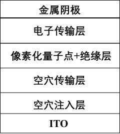
QNED displays utilize quantum dot structures to enhance display performance. These structures typically consist of a core-shell configuration, where the core material is responsible for light emission and the shell provides protection and improves efficiency. The quantum dots are often made from semiconductor materials and can be precisely tuned to emit specific colors, contributing to improved color accuracy and resolution in QNED displays.- QNED display structure and composition: QNED displays utilize quantum nano-emitting diodes, which are composed of nanoscale semiconductor materials. These displays incorporate quantum dot technology to enhance color performance and brightness. The structure typically includes multiple layers such as electron transport layers, hole transport layers, and emissive layers containing quantum dots.
- Resolution enhancement techniques: Various methods are employed to improve the resolution of QNED displays. These include optimizing pixel arrangements, developing advanced driving circuits, and implementing sub-pixel rendering techniques. Some approaches focus on reducing the size of individual quantum dots while maintaining their emission efficiency to achieve higher pixel densities.
- Color gamut and brightness improvements: QNED displays aim to achieve wider color gamuts and higher brightness levels compared to conventional display technologies. This is accomplished through the precise control of quantum dot size and composition, as well as the development of more efficient light extraction methods. Some designs incorporate color filters or utilize multi-primary color systems to further enhance color reproduction.
- Energy efficiency and power consumption: Researchers are focusing on improving the energy efficiency of QNED displays to reduce power consumption. This involves optimizing the quantum yield of the emitting materials, developing more efficient electron injection and transport layers, and implementing advanced power management systems. Some designs also explore the use of micro-LED backlight units to further enhance energy efficiency.
- Manufacturing processes and scalability: Advancements in manufacturing processes are crucial for the commercialization of high-resolution QNED displays. This includes developing scalable methods for quantum dot synthesis and deposition, improving the uniformity of quantum dot layers, and enhancing the overall yield of the production process. Some approaches explore the integration of QNED technology with existing display manufacturing infrastructure to facilitate mass production.
02 Nano-scale emitting diodes in QNED technology
QNED displays incorporate nano-scale emitting diodes, which are significantly smaller than traditional LED structures. These nano-scale diodes allow for higher pixel density and improved resolution. The miniaturization of emitting diodes enables more precise control over light emission, resulting in sharper images and better overall display quality.Expand Specific Solutions03 Color conversion and light management in QNED displays
QNED technology employs advanced color conversion techniques and light management systems to achieve high resolution and color accuracy. This includes the use of color filters, quantum dot color converters, and specialized optical structures to enhance light extraction and directionality. These components work together to improve color gamut, contrast, and overall image quality in QNED displays.Expand Specific Solutions04 Fabrication methods for high-resolution QNED displays
Various fabrication techniques are employed to produce high-resolution QNED displays. These methods include advanced lithography processes, selective area growth of quantum dots, and precise deposition techniques for creating nano-scale structures. The fabrication processes focus on achieving uniform and densely packed quantum dot arrays, which are crucial for high-resolution display performance.Expand Specific Solutions05 Integration of QNED technology with existing display architectures
QNED technology is being integrated with existing display architectures to enhance resolution and overall performance. This integration involves combining quantum dot and nano-emitting diode technologies with traditional display components such as TFT backplanes and color filters. The result is a hybrid display technology that leverages the strengths of multiple approaches to achieve superior resolution and image quality.Expand Specific Solutions
Key QNED Players
The competition landscape for achieving high-resolution displays with QNED is in its early development stage, with significant potential for market growth. The technology is still emerging, with major players like Samsung Display, LG Display, and BOE Technology Group leading research efforts. These companies are investing heavily in QNED development, recognizing its potential to revolutionize display technology. The market size is expected to expand rapidly as QNED offers superior image quality and energy efficiency compared to existing technologies. While not yet fully mature, QNED is progressing quickly, with companies like Sharp, TCL, and Tianma Microelectronics also entering the field, indicating a competitive and dynamic landscape poised for significant advancements in the near future.
BOE Technology Group Co., Ltd.
Technical Solution: BOE is actively researching and developing QNED technology as part of its next-generation display portfolio. Their approach focuses on creating self-emissive quantum dot displays that can achieve higher brightness and wider color gamut than OLED. BOE's QNED technology uses inorganic semiconductor nanorods as the light-emitting material, which are then combined with quantum dots for color conversion. The company has demonstrated prototype QNED displays with improved efficiency and longevity compared to organic light-emitting materials. BOE is also exploring the integration of QNED with flexible and transparent display technologies.
Strengths: Strong position in the display market, experience with various display technologies, and potential for cost-effective production. Weaknesses: Still in early stages of QNED development compared to some competitors.
Samsung Display Co., Ltd.
Technical Solution: Samsung Display has developed a QNED (Quantum Nano Emitting Diode) technology that combines quantum dot and nanorod LED technologies. Their approach uses ultra-small LEDs as the light source, with each pixel composed of red, green, and blue nanorods. These nanorods are coated with quantum dots to enhance color purity and efficiency. The company has demonstrated prototypes with pixel densities exceeding 10,000 PPI, showcasing the potential for extremely high-resolution displays.
Strengths: Extremely high pixel density, superior color accuracy, and potential for high energy efficiency. Weaknesses: Complex manufacturing process and potentially high production costs in the early stages of commercialization.
QNED Core Innovations
High-performance ultrahigh-resolution QLED prepared by one-step transfer printing
PatentActiveCN113937230A
Innovation
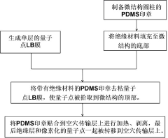
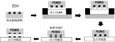
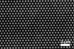
- One-step transfer printing technology is used to combine quantum dot LB film and PDMS stamp, and by embedding insulating material between quantum dot pixels as a current blocking layer, reducing the pixel size and solving the leakage current problem, a high-performance ultra-high resolution QLED is prepared.
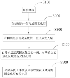
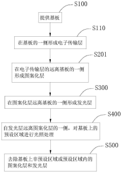
Method for preparing QLED device, QLED device and display device
PatentActiveCN113903874B
Innovation
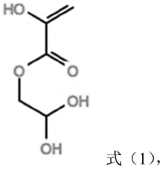
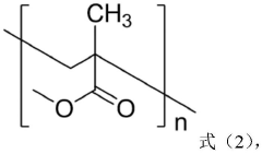
- Use small molecule cross-linked materials and polymer decomposition materials to form a patterned layer, change the solubility through light treatment, remove the patterned layer and luminescent layer in non-preset areas, prepare high-resolution QLED devices, and use the patterned layer as a Electron blocking layers improve device performance.
QNED Manufacturing
QNED (Quantum Nano-Emitting Diode) manufacturing represents a critical aspect of achieving high-resolution displays with this emerging technology. The production process for QNED displays involves several complex steps and requires advanced manufacturing techniques to ensure the quality and performance of the final product.
The fabrication of QNED displays begins with the preparation of the quantum dot material, which forms the basis of the nano-emitting diodes. This process involves precise control of quantum dot size and composition to achieve the desired emission wavelengths for red, green, and blue light. The quantum dots are typically synthesized using colloidal chemistry methods, requiring careful temperature and reaction time control.
Once the quantum dots are prepared, they are integrated into a matrix material to form the emissive layer. This step often involves the use of advanced deposition techniques such as inkjet printing or photolithography to achieve precise patterning of the quantum dot layers. The accuracy and uniformity of this deposition process are crucial for ensuring consistent color reproduction across the display.
The next stage in QNED manufacturing involves the fabrication of the nanorod LED structures. These nanorods serve as the electron injection and transport layers, working in conjunction with the quantum dot emissive layer. The growth of these nanorod structures typically employs epitaxial techniques such as molecular beam epitaxy (MBE) or metal-organic chemical vapor deposition (MOCVD).
Following the nanorod growth, the QNED structure is completed by depositing additional layers for hole transport and electrode contacts. These layers are often applied using physical vapor deposition (PVD) or chemical vapor deposition (CVD) techniques. The precise thickness and composition of these layers are critical for optimizing the electrical and optical properties of the QNED device.
One of the key challenges in QNED manufacturing is achieving high uniformity and yield across large-area displays. This requires careful process control and optimization at each stage of production. Advanced in-line monitoring and quality control systems are typically employed to ensure consistency and detect defects early in the manufacturing process.
Another important aspect of QNED manufacturing is the integration of the QNED elements into a complete display module. This involves the assembly of the QNED panel with driving electronics, backlighting systems (if required), and protective layers. The final assembly process must be carried out in a clean room environment to prevent contamination and ensure the longevity of the display.
QNED vs. Competitors
QNED (Quantum Nano Emitting Diode) technology represents a significant advancement in display technology, offering several advantages over its competitors in the high-resolution display market. When compared to traditional LCD and OLED displays, QNED exhibits superior performance in key areas such as brightness, color accuracy, and energy efficiency.
One of the primary advantages of QNED over LCD technology is its ability to achieve higher contrast ratios and deeper blacks. Unlike LCD displays that rely on backlighting, QNED uses self-emissive quantum dots, allowing for precise control of individual pixels. This results in improved local dimming capabilities and enhanced overall picture quality.
In comparison to OLED displays, QNED offers better longevity and resistance to burn-in issues. The inorganic nature of quantum dots used in QNED technology makes them less susceptible to degradation over time, addressing one of the main concerns associated with OLED displays.
QNED also outperforms both LCD and OLED in terms of color gamut and accuracy. The quantum dot technology enables QNED displays to produce a wider range of colors with greater precision, resulting in more vibrant and lifelike images. This makes QNED particularly attractive for applications requiring high color fidelity, such as professional content creation and high-end consumer electronics.
Energy efficiency is another area where QNED shows promise. The technology's ability to emit light directly from quantum dots reduces power consumption compared to LCD displays, which require constant backlighting. While OLED displays are also energy-efficient, QNED has the potential to surpass them in this aspect, especially at higher brightness levels.
In terms of manufacturing scalability, QNED holds an advantage over OLED technology. The production process for QNED displays is more compatible with existing LCD manufacturing infrastructure, potentially leading to lower production costs and faster market adoption.
However, QNED is not without its challenges. The technology is still in its early stages of development, and mass production hurdles need to be overcome. Additionally, while QNED offers improvements in many areas, it may not completely outperform OLED in all aspects, such as response time and viewing angles.
As the display industry continues to evolve, QNED technology positions itself as a strong contender in the high-resolution display market. Its unique combination of advantages over both LCD and OLED technologies makes it a promising solution for next-generation displays, particularly in applications where image quality, longevity, and energy efficiency are paramount.
Unlock deeper insights with Patsnap Eureka Quick Research — get a full tech report to explore trends and direct your research. Try now!
Generate Your Research Report Instantly with AI Agent
Supercharge your innovation with Patsnap Eureka AI Agent Platform!