QNED for Enhanced Optical Performance in Displays
JUN 19, 20259 MIN READ
Generate Your Research Report Instantly with AI Agent
Patsnap Eureka helps you evaluate technical feasibility & market potential.
QNED Technology Evolution
QNED (Quantum Nano Emitting Diode) technology has undergone significant evolution since its inception, marking a revolutionary advancement in display technology. The journey of QNED began with the fundamental research on quantum dot materials and their potential application in light-emitting devices.
In the early stages, researchers focused on developing stable quantum dot materials that could emit light efficiently. This phase involved extensive experimentation with various semiconductor nanocrystals, particularly those based on cadmium selenide (CdSe) and indium phosphide (InP). The primary challenge was to achieve precise control over the size and composition of these nanocrystals, as these factors directly influence the color and quality of emitted light.
As the understanding of quantum dot behavior improved, the next phase of QNED evolution centered on integrating these nanocrystals into functional display structures. This period saw the development of methods to deposit quantum dots onto substrates and create multi-layer structures that could effectively convert electrical energy into light. Researchers explored various deposition techniques, including spin-coating, inkjet printing, and photolithography, to achieve uniform and precise quantum dot layers.
A significant milestone in QNED evolution was the development of blue self-emissive quantum dots. While red and green quantum dots had been relatively easy to produce, blue-emitting dots posed a considerable challenge due to their higher energy requirements. The breakthrough in blue quantum dots opened the door for full-color QNED displays, marking a crucial step towards commercial viability.
The next phase focused on enhancing the stability and longevity of QNED devices. Early prototypes suffered from rapid degradation due to oxidation and other environmental factors. Researchers developed advanced encapsulation techniques and protective layers to shield the quantum dots from external influences, significantly improving device lifetimes.
Recent advancements in QNED technology have centered on improving efficiency and color purity. This has involved refining the quantum dot synthesis process to achieve narrower emission spectra, resulting in more vibrant and accurate colors. Additionally, efforts have been made to reduce energy consumption by optimizing the electron transport layers and developing more efficient driving circuits.
The latest frontier in QNED evolution is the exploration of cadmium-free quantum dots to address environmental concerns. This has led to increased research into indium-based and perovskite quantum dots, which show promising results in terms of performance and eco-friendliness.
Throughout its evolution, QNED technology has consistently aimed to surpass the limitations of existing display technologies, offering superior color gamut, brightness, and energy efficiency. The ongoing research continues to push the boundaries of what is possible in display technology, with QNED poised to play a significant role in the next generation of high-performance displays.
Display Market Trends
The display market has been experiencing significant growth and transformation in recent years, driven by technological advancements and changing consumer preferences. The global display market size reached $148 billion in 2021 and is projected to grow at a CAGR of 6.2% from 2022 to 2030. This growth is primarily fueled by the increasing demand for high-quality displays across various sectors, including consumer electronics, automotive, and healthcare.
One of the most notable trends in the display market is the shift towards higher resolution and larger screen sizes. 4K and 8K displays are gaining traction, particularly in the premium segment of the market. The demand for larger screens is also on the rise, with consumers showing a preference for immersive viewing experiences. This trend is evident in both the television and smartphone markets, where manufacturers are pushing the boundaries of screen-to-body ratios.
Another significant trend is the adoption of advanced display technologies. OLED displays have seen substantial growth, particularly in smartphones and high-end televisions, due to their superior color reproduction and contrast ratios. However, the high cost of OLED production has led to the development of alternative technologies like QLED and MicroLED, which aim to offer similar performance at a lower cost.
The automotive sector is emerging as a key growth driver for the display market. The increasing integration of infotainment systems and digital dashboards in vehicles is creating new opportunities for display manufacturers. Additionally, the rise of electric and autonomous vehicles is expected to further boost the demand for advanced displays in the automotive industry.
Sustainability and energy efficiency have become important considerations in the display market. Manufacturers are focusing on developing eco-friendly display technologies that consume less power and use sustainable materials. This trend aligns with global efforts to reduce carbon emissions and promote environmental responsibility.
The COVID-19 pandemic has had a significant impact on the display market. While it initially disrupted supply chains and manufacturing processes, it also led to increased demand for displays in remote work and education settings. This shift has accelerated the adoption of larger, higher-quality displays for home use.
Looking ahead, emerging technologies like flexible and foldable displays are expected to shape the future of the market. These innovations open up new possibilities for device form factors and user experiences. Additionally, the development of quantum dot technology, including QNED (Quantum Nano Emitting Diode), holds promise for enhancing optical performance in displays, potentially offering improved color accuracy, brightness, and energy efficiency.
QNED Technical Challenges
QNED (Quantum Nano Emitting Diode) technology faces several significant technical challenges in its development and implementation for enhanced optical performance in displays. One of the primary hurdles is achieving consistent and uniform quantum dot synthesis. The size and composition of quantum dots directly impact their emission wavelength and efficiency, making precise control over their production crucial for display applications.
Another major challenge lies in the integration of quantum dots with existing LED structures. The interface between the quantum dot layer and the LED substrate must be carefully engineered to ensure efficient energy transfer and minimize losses. This integration process requires advanced manufacturing techniques and materials science expertise to optimize the overall device performance.
Stability and longevity of QNED displays present ongoing concerns. Quantum dots can be sensitive to environmental factors such as heat, moisture, and oxygen, which can lead to degradation over time. Developing robust encapsulation methods and protective layers to shield the quantum dots from these external factors is essential for ensuring the long-term reliability of QNED displays.
Color accuracy and gamut expansion remain critical areas for improvement. While QNED technology promises superior color reproduction compared to traditional LED displays, achieving precise color control across a wide range of viewing conditions is challenging. Fine-tuning the emission spectra of quantum dots and optimizing color filters are necessary steps to fully realize the potential of QNED in expanding the color gamut.
Power efficiency is another key consideration in QNED development. Although quantum dots offer the potential for improved energy efficiency, optimizing the overall system to minimize power consumption while maintaining high brightness and color quality requires careful balancing of various components and materials.
Scaling up production for commercial viability presents significant manufacturing challenges. Developing cost-effective, high-volume production methods for quantum dots and integrating them into display manufacturing processes without compromising quality or performance is crucial for widespread adoption of QNED technology.
Addressing blue light emission remains a persistent challenge. While red and green quantum dots have shown promising results, achieving stable and efficient blue emission has proven more difficult. Overcoming this hurdle is essential for creating full-color QNED displays with balanced performance across all primary colors.
Current QNED Solutions
01 Quantum dot structure and composition
QNED devices utilize quantum dots with specific structures and compositions to enhance optical performance. These quantum dots are typically made of semiconductor materials and can be engineered to emit light at specific wavelengths. The size, shape, and material composition of the quantum dots play crucial roles in determining the optical properties of the QNED device.- Quantum dot structure and composition: QNED devices utilize quantum dots with specific structures and compositions to enhance optical performance. These quantum dots are typically made of semiconductor materials and are engineered to have precise sizes and shapes. The composition and structure of the quantum dots directly influence the emission wavelength and efficiency of the QNED device.
- Light-emitting layer design: The design of the light-emitting layer in QNED devices is crucial for optimal optical performance. This includes the arrangement of quantum dots, the use of multiple quantum well structures, and the incorporation of barrier layers. The light-emitting layer design affects the electron-hole recombination efficiency and the overall light output of the device.
- Electrode and contact optimization: The optimization of electrodes and electrical contacts in QNED devices is essential for efficient current injection and light extraction. This involves the use of transparent conductive materials, patterned electrodes, and advanced contact designs to minimize resistance and maximize light output. Proper electrode design also contributes to improved device stability and longevity.
- Encapsulation and packaging techniques: Advanced encapsulation and packaging techniques are employed to protect QNED devices from environmental factors and enhance their optical performance. These techniques include the use of hermetic seals, moisture barriers, and optical coatings. Proper encapsulation helps maintain the stability of quantum dots and prevents degradation of the device's optical properties over time.
- Integration with optical components: QNED devices are often integrated with additional optical components to further enhance their performance. This may include the use of micro-lenses, photonic crystals, or plasmonic structures to improve light extraction and directionality. The integration of these components can significantly boost the overall optical efficiency and output of QNED-based displays or lighting systems.
02 Light emission and color control
QNEDs offer precise control over light emission and color output. By manipulating the quantum dot properties and device structure, researchers can achieve a wide color gamut and high color purity. This enables the production of displays with vibrant and accurate colors, as well as the ability to fine-tune the emission spectrum for specific applications.Expand Specific Solutions03 Efficiency and brightness enhancement
Various techniques are employed to improve the efficiency and brightness of QNED devices. These may include optimizing the quantum dot layer structure, incorporating light extraction features, and enhancing charge carrier injection and transport. Such improvements lead to higher luminous efficacy and brighter displays.Expand Specific Solutions04 Integration with display technologies
QNED technology can be integrated with existing display technologies to enhance overall performance. This includes combining quantum dots with LED backlights, incorporating them into OLED structures, or developing hybrid display architectures. Such integrations aim to leverage the strengths of multiple technologies for superior optical performance.Expand Specific Solutions05 Stability and lifetime improvement
Enhancing the stability and lifetime of QNED devices is crucial for their practical application. Research focuses on developing encapsulation techniques, improving quantum dot stability, and optimizing device structures to prevent degradation. These efforts aim to ensure consistent optical performance over extended periods of operation.Expand Specific Solutions
Key QNED Industry Players
The research on QNED for enhanced optical performance in displays is currently in an emerging stage, with significant potential for market growth. The global display market, valued at over $150 billion, is witnessing a shift towards advanced technologies like QNED. While the technology is still maturing, major players such as Samsung Display, BOE Technology, and Sharp are investing heavily in R&D. Companies like TCL China Star Optoelectronics and LG Display are also making strides in QNED development. The competitive landscape is characterized by a mix of established display manufacturers and innovative startups, with collaborations between industry and academia, such as partnerships involving The Hong Kong University of Science & Technology, driving technological advancements. As QNED technology progresses, it is expected to challenge existing display technologies, potentially reshaping the market dynamics in the coming years.
BOE Technology Group Co., Ltd.
Technical Solution: BOE has been actively researching QNED technology to enhance optical performance in displays. Their approach focuses on integrating quantum dot nanoparticles with miniLED backlighting systems. This hybrid technology aims to combine the advantages of quantum dots' color performance with the high brightness and local dimming capabilities of miniLEDs. BOE's QNED displays are designed to offer improved color gamut, higher contrast ratios, and better HDR performance compared to traditional LCD displays. The company is working on optimizing the quantum dot layer and developing advanced light management films to maximize the benefits of this technology.
Strengths: Potential for high brightness and wide color gamut, leveraging existing LCD manufacturing infrastructure. Weaknesses: Complexity in aligning quantum dots with miniLED backlights, potential for color shift at wide viewing angles.
Sharp Corp.
Technical Solution: Sharp has been conducting research on QNED technology to improve optical performance in displays. Their approach focuses on combining quantum dot technology with micro-LED backlighting systems. Sharp's QNED displays aim to achieve higher brightness, wider color gamut, and improved contrast ratios compared to conventional LCD and OLED technologies. The company is working on developing precise quantum dot deposition techniques and optimizing the interaction between quantum dots and micro-LEDs to maximize light output and color purity. Sharp is also exploring ways to enhance the stability and longevity of quantum dot materials in display applications.
Strengths: Potential for high brightness and wide color gamut, leveraging Sharp's expertise in LCD technology. Weaknesses: Challenges in achieving cost-effective production of micro-LED backlight systems, potential issues with quantum dot degradation over time.
QNED Core Innovations
Quantum-nano light emitting diode pixel and quantum-nano light emitting diode display device
PatentActiveUS20190081261A1
Innovation
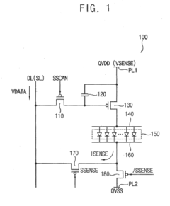
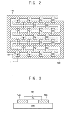
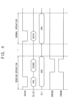
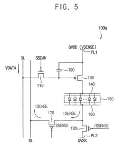
- A Q-NED pixel and display device design that includes a switching transistor, storage capacitor, driving transistor, and sensing transistors to sense and compensate for ohmic contact resistance deviations, utilizing inorganic materials like gallium nitride for the Q-NEDs, with anode and cathode electrodes having a comb shape to enhance light emission efficiency and maintain luminance over time.
Quantum dot color filter substrate, fabricating method thereof, and display panel
PatentActiveUS20210336171A1
Innovation
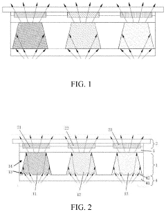
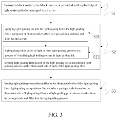
- A quantum dot color filter substrate with light-guiding grooves and protrusions on the surface of light-guiding films, which act as convex mirrors to increase the optical path of incident light, reducing absorption by the black matrix and enhancing light utilization efficiency without increasing the luminous intensity of the light-emitting device.
QNED Manufacturing Process
The QNED (Quantum Nano Emitting Diode) manufacturing process represents a significant advancement in display technology, combining the benefits of quantum dots and mini-LED backlighting. This process involves several intricate steps to achieve the enhanced optical performance characteristic of QNED displays.
The foundation of QNED manufacturing lies in the production of quantum dots, typically composed of semiconductor nanocrystals. These quantum dots are synthesized through precise chemical processes, controlling their size and composition to achieve specific light emission properties. The quantum dots are then integrated into a film or layer that will serve as the color conversion element in the display.
Concurrently, the mini-LED backlight units are manufactured. This process involves the production of extremely small LED chips, typically measuring less than 200 micrometers. These mini-LEDs are fabricated using advanced semiconductor manufacturing techniques, including epitaxial growth, photolithography, and etching processes. The mini-LEDs are then precisely placed on a substrate to form the backlight array.
The integration of the quantum dot layer with the mini-LED backlight is a critical step in QNED manufacturing. This involves carefully aligning and bonding the quantum dot film to the mini-LED array, ensuring optimal light transmission and color conversion. Advanced placement techniques and bonding methods are employed to achieve the necessary precision and durability.
The next phase involves the assembly of the liquid crystal layer, which modulates the light from the quantum dot-enhanced mini-LED backlight. This requires clean room conditions and specialized equipment to ensure uniform distribution of the liquid crystal material and proper alignment with the other layers of the display.
Finally, the display panel is completed with the addition of color filters, polarizers, and the front glass or plastic substrate. These components are carefully aligned and bonded to create the final QNED display structure. Throughout the manufacturing process, stringent quality control measures are implemented to ensure consistency in color reproduction, brightness, and overall display performance.
The QNED manufacturing process also incorporates various optimization techniques to enhance optical performance. These may include the use of light-guiding structures, optical films to improve light distribution, and advanced driving circuits to control the mini-LED backlight with high precision. Additionally, the process may involve the application of anti-reflection coatings and other surface treatments to improve display visibility and reduce glare.
QNED Energy Efficiency
QNED (Quantum Nano Emitting Diode) technology has shown significant potential in enhancing the energy efficiency of display systems. The energy efficiency of QNED displays is primarily attributed to their unique structure and operational mechanisms, which allow for improved light emission and reduced power consumption compared to traditional display technologies.
QNED displays utilize quantum dots as the light-emitting material, which are semiconductor nanocrystals that can emit light with high efficiency and color purity. These quantum dots are typically embedded in a matrix of nanorod LEDs, creating a hybrid structure that combines the benefits of both technologies. The quantum dots can be precisely tuned to emit specific wavelengths of light, resulting in highly saturated colors and a wider color gamut.
One of the key factors contributing to the energy efficiency of QNED displays is their ability to produce light directly at the desired wavelengths. Unlike traditional LCD displays that require color filters to produce different colors, QNED displays can generate pure red, green, and blue light without the need for additional filtering. This direct emission approach significantly reduces energy losses associated with color conversion and filtering processes.
Furthermore, QNED displays exhibit improved light extraction efficiency compared to conventional LED displays. The nanorod structure of the LEDs allows for better light outcoupling, reducing internal reflections and increasing the overall light output. This enhanced light extraction translates to higher brightness levels while consuming less power, contributing to the overall energy efficiency of the display.
The quantum dot layer in QNED displays also plays a crucial role in energy efficiency. Quantum dots have a high quantum yield, meaning they can convert a large portion of the input energy into light with minimal losses. This high conversion efficiency results in less heat generation and lower power consumption compared to traditional phosphor-based LED displays.
Additionally, QNED displays benefit from the ability to implement local dimming techniques more effectively. The nanorod LED structure allows for precise control over individual pixels or small groups of pixels, enabling dynamic contrast adjustment and selective dimming of dark areas. This localized control further enhances energy efficiency by reducing power consumption in areas of the display that do not require high brightness.
The combination of these factors results in QNED displays achieving higher luminous efficacy, measured in lumens per watt, compared to conventional display technologies. This improved efficiency translates to reduced power consumption and longer battery life in portable devices, as well as lower energy costs for larger display installations.
Unlock deeper insights with Patsnap Eureka Quick Research — get a full tech report to explore trends and direct your research. Try now!
Generate Your Research Report Instantly with AI Agent
Supercharge your innovation with Patsnap Eureka AI Agent Platform!