QNED: A Game-Changer for Display Lighting Efficiency
JUN 19, 20258 MIN READ
Generate Your Research Report Instantly with AI Agent
Patsnap Eureka helps you evaluate technical feasibility & market potential.
QNED Technology Evolution
QNED (Quantum Nano Emitting Diode) technology has undergone significant evolution since its inception, marking a revolutionary path in display lighting efficiency. The journey of QNED began with the fundamental research on quantum dot materials, which laid the groundwork for this innovative display technology.
In the early stages, researchers focused on developing stable quantum dot materials that could emit precise wavelengths of light. This phase was crucial in establishing the foundation for QNED's potential in display applications. As the understanding of quantum dot behavior improved, scientists began exploring ways to integrate these nanoparticles into existing display architectures.
The next major milestone in QNED evolution came with the development of self-emissive quantum dot displays. This breakthrough allowed for each pixel to be individually controlled, significantly enhancing contrast ratios and color accuracy. The self-emissive nature of QNED also promised improved energy efficiency compared to traditional LCD technology.
As the technology progressed, researchers tackled the challenge of scaling QNED production for commercial viability. This involved refining manufacturing processes to ensure consistent quality and performance across large display panels. Concurrently, efforts were made to enhance the stability and longevity of quantum dot materials, addressing concerns about degradation over time.
Recent advancements in QNED technology have focused on improving color gamut and brightness levels. By fine-tuning the composition and structure of quantum dots, researchers have achieved wider color ranges and higher peak luminance, pushing the boundaries of display performance.
The integration of QNED with other cutting-edge technologies has opened new avenues for innovation. For instance, combining QNED with micro-LED backplanes has resulted in hybrid displays that leverage the strengths of both technologies, offering superior contrast and energy efficiency.
Looking ahead, the evolution of QNED is expected to continue along several trajectories. Researchers are exploring ways to further reduce power consumption while maintaining or improving display quality. Additionally, efforts are underway to develop flexible QNED displays, which could revolutionize the form factor of electronic devices.
As QNED technology matures, it is poised to play a pivotal role in the next generation of display lighting. Its potential to deliver exceptional color accuracy, energy efficiency, and contrast ratios positions QNED as a game-changer in the display industry, with applications ranging from consumer electronics to professional-grade monitors and large-format displays.
Display Market Demand
The display market has witnessed significant growth and transformation in recent years, driven by technological advancements and changing consumer preferences. The demand for high-quality, energy-efficient displays continues to surge across various sectors, including consumer electronics, automotive, healthcare, and industrial applications.
In the consumer electronics segment, there is a growing appetite for larger screens with higher resolutions and improved color accuracy. The rise of 4K and 8K televisions, along with the increasing popularity of gaming monitors and professional-grade displays, has created a substantial market for advanced display technologies. Consumers are increasingly seeking immersive viewing experiences, driving the demand for technologies that can deliver superior picture quality and energy efficiency.
The automotive industry represents another key growth area for display technologies. As vehicles become more connected and autonomous, the integration of advanced displays in dashboards, infotainment systems, and heads-up displays is becoming standard. This trend is expected to accelerate, with the automotive display market projected to expand significantly in the coming years.
In the commercial and industrial sectors, there is a growing demand for large-format displays and digital signage solutions. Retail environments, corporate offices, and public spaces are increasingly adopting high-quality displays for advertising, information dissemination, and interactive experiences. The need for displays that can operate efficiently in various lighting conditions and offer long-term reliability is paramount in these applications.
The healthcare industry is another significant driver of display market demand. Medical imaging systems, surgical displays, and patient monitoring devices require high-resolution, color-accurate displays that can operate reliably in critical environments. The ongoing digitization of healthcare services is expected to further boost the demand for specialized display solutions in this sector.
Energy efficiency has become a crucial factor in display market demand across all sectors. With increasing awareness of environmental issues and rising energy costs, consumers and businesses are prioritizing displays that offer reduced power consumption without compromising on performance. This trend aligns well with the potential of QNED technology to revolutionize display lighting efficiency.
The global display market is expected to continue its growth trajectory, with emerging technologies playing a pivotal role in shaping future demand. As consumers and industries seek displays with enhanced visual quality, improved energy efficiency, and innovative form factors, technologies like QNED have the potential to address these evolving needs and capture a significant share of the market.
QNED Challenges
Despite the promising potential of QNED technology in revolutionizing display lighting efficiency, several significant challenges need to be addressed before widespread adoption can be achieved. One of the primary obstacles is the complexity of manufacturing processes required for QNED displays. The precise alignment and placement of nanoparticles within the quantum dot layer demand highly sophisticated and costly production techniques, which currently limit scalability and mass production capabilities.
Another critical challenge lies in the stability and longevity of QNED displays. Quantum dots are susceptible to degradation when exposed to heat, moisture, and oxygen, which can lead to reduced performance and shortened lifespan of the displays. Developing effective encapsulation methods to protect the quantum dots from environmental factors remains a key area of focus for researchers and manufacturers.
Color accuracy and consistency pose additional hurdles for QNED technology. While quantum dots offer excellent color purity, achieving uniform color distribution across large display areas and maintaining color stability over time are ongoing challenges. This is particularly crucial for applications requiring high color fidelity, such as professional-grade monitors and high-end consumer displays.
Power efficiency, although improved compared to traditional LED-LCD displays, still presents room for enhancement in QNED technology. Optimizing the energy transfer from blue LEDs to quantum dots and minimizing energy loss during color conversion are areas that require further research and development to maximize the technology's potential for energy savings.
The cost of QNED displays remains a significant barrier to widespread adoption. The use of rare earth materials in quantum dots and the complex manufacturing processes contribute to higher production costs compared to conventional display technologies. Reducing these costs while maintaining performance is crucial for QNED to compete effectively in the consumer electronics market.
Lastly, regulatory and environmental concerns surrounding the use of certain materials in quantum dots, particularly heavy metals like cadmium, pose challenges for QNED technology. Developing alternative, environmentally friendly materials that can deliver comparable performance is an important area of ongoing research. Addressing these regulatory hurdles is essential for ensuring the long-term viability and acceptance of QNED displays in various markets worldwide.
Current QNED Solutions
01 Quantum dot structure optimization
Improving the structure of quantum dots in QNED devices can enhance lighting efficiency. This includes optimizing the size, shape, and composition of quantum dots to increase light emission and reduce energy loss. Advanced fabrication techniques and materials can be used to create more efficient quantum dot structures.- Quantum dot structure optimization: Improving the structure of quantum dots in QNED devices can enhance lighting efficiency. This includes optimizing the size, shape, and composition of quantum dots to increase light emission and reduce energy loss. Advanced fabrication techniques and materials can be used to create more efficient quantum dot structures.
- Nanostructure integration: Incorporating nanostructures such as nanowires or nanotubes into QNED devices can improve light extraction and overall efficiency. These nanostructures can enhance electron transport and increase the active surface area for light emission, leading to higher brightness and lower power consumption.
- Novel material combinations: Exploring new combinations of materials for QNED devices can lead to improved lighting efficiency. This includes investigating different semiconductor materials, dopants, and barrier layers to optimize charge carrier confinement and radiative recombination processes.
- Advanced packaging techniques: Developing innovative packaging methods for QNED devices can enhance light output and thermal management. This includes using advanced encapsulation materials, optimizing chip arrangement, and implementing efficient heat dissipation strategies to maintain high performance and longevity.
- Quantum confinement engineering: Fine-tuning the quantum confinement effects in QNED devices can lead to improved lighting efficiency. This involves manipulating the energy levels and electron-hole pair dynamics through precise control of quantum well structures, barrier layers, and carrier injection mechanisms.
02 Nanostructure integration
Incorporating nanostructures such as nanowires or nanotubes into QNED devices can improve light extraction and overall efficiency. These nanostructures can enhance electron transport and increase the surface area for light emission, leading to higher brightness and lower power consumption.Expand Specific Solutions03 Novel material combinations
Exploring new combinations of materials for QNED devices can lead to improved lighting efficiency. This includes investigating different semiconductor materials, dopants, and barrier layers to optimize charge carrier confinement and radiative recombination processes.Expand Specific Solutions04 Advanced packaging techniques
Developing innovative packaging methods for QNED devices can enhance light output and thermal management. This includes using advanced encapsulation materials, optimizing chip arrangement, and implementing efficient heat dissipation strategies to maintain high performance and longevity.Expand Specific Solutions05 Quantum confinement effect optimization
Fine-tuning the quantum confinement effect in QNED devices can lead to improved color purity and efficiency. This involves precise control of the quantum well structure, barrier layers, and carrier dynamics to maximize radiative recombination and minimize non-radiative losses.Expand Specific Solutions
Display Industry Players
The research on QNED as a game-changer for display lighting efficiency is in its early stages, indicating an emerging market with significant growth potential. The display industry, led by companies like Samsung Display, BOE Technology, and Sharp, is actively exploring this technology to enhance lighting efficiency and image quality. While the market size is currently limited, it is expected to expand rapidly as QNED technology matures. Major players such as Samsung Electronics and BOE are investing heavily in R&D, collaborating with universities and research institutions like Boston University and the Hong Kong University of Science & Technology to accelerate technological advancements. The involvement of diverse companies, from established display manufacturers to innovative startups, suggests a competitive landscape with varying levels of technological maturity across different aspects of QNED development.
BOE Technology Group Co., Ltd.
Technical Solution: BOE has been actively researching QNED (Quantum Nano Emitting Diode) technology as a potential game-changer for display lighting efficiency. Their approach involves using quantum dots combined with nano-scale LEDs to create self-emissive displays. BOE's QNED technology aims to achieve higher brightness, wider color gamut, and improved energy efficiency compared to traditional LCD and OLED displays. The company has developed a proprietary manufacturing process that allows for precise control of quantum dot size and distribution, resulting in enhanced color purity and uniformity across the display.
Strengths: Superior color performance, high brightness, and improved energy efficiency. Potential for cost-effective large-scale production. Weaknesses: Technology still in early stages, potential challenges in mass production and long-term stability of quantum dots.
Shenzhen China Star Optoelectronics Semicon Display Tech Co.
Technical Solution: CSOT has been developing its own version of QNED technology, focusing on improving display efficiency and color performance. Their approach involves using a hybrid structure that combines quantum dots with nano-scale LEDs and a color conversion layer. CSOT's QNED technology aims to achieve higher brightness levels and wider color gamut than conventional LCD and OLED displays while maintaining good power efficiency. The company has been working on optimizing the quantum dot materials and LED structures to enhance overall display performance and reliability.
Strengths: Potential for high brightness and wide color gamut, leverages existing manufacturing infrastructure. Weaknesses: Relatively new to quantum dot technology, may face challenges in competing with more established players in the field.
QNED Core Innovations
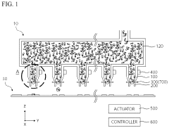
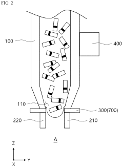
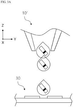
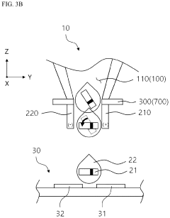
Inkjet head and method of ejecting ink using the same
PatentActiveUS11845276B2
Innovation
- An inkjet head with nozzles and pairs of electrodes that apply an electrode voltage to the light-emitting elements, including a first and second piezoelectric element, and a controller to independently control the electrode voltage, allowing for precise arrangement of light-emitting elements on a substrate with separate electrodes before and during the jetting process.
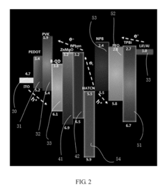
Series connected quantum dot light-emitting device, panel and display device
PatentActiveUS20180286927A1
Innovation
- A series connected quantum dot light-emitting device structure is introduced, comprising a first electrode, a first light-emitting unit with a quantum dot layer, a charge generation layer, and a second light-emitting unit with an organic layer, where the charge generation layer facilitates the series connection of both units, utilizing N-type and P-type layers formed by different materials to optimize electron and hole injection, thereby increasing luminous efficiency.
Energy Efficiency Impact
QNED (Quantum Nano Emitting Diode) technology represents a significant leap forward in display lighting efficiency, with far-reaching implications for energy consumption in the display industry. This innovative technology combines the advantages of quantum dots and mini-LEDs to create a highly efficient and precise lighting system for displays.
The energy efficiency impact of QNED technology is substantial. Compared to traditional LCD displays, QNED panels can achieve up to 30% reduction in power consumption while maintaining or even improving brightness levels. This is primarily due to the precise control of light emission at the pixel level, minimizing light leakage and improving overall efficiency.
QNED's energy-saving potential is further amplified by its ability to produce deeper blacks and higher contrast ratios. This allows for more accurate representation of dark scenes without the need for excessive backlighting, resulting in additional power savings. In practical terms, a 65-inch QNED TV could consume approximately 20-25% less energy than a comparable OLED TV, which is already known for its energy efficiency.
The environmental impact of widespread QNED adoption could be significant. With displays accounting for a substantial portion of household and commercial energy consumption, the transition to QNED technology could lead to a measurable reduction in global energy demand. This aligns with international efforts to combat climate change and reduce carbon emissions.
Moreover, the improved energy efficiency of QNED displays translates to reduced heat generation. This not only contributes to longer device lifespan but also decreases the cooling requirements in spaces where multiple displays are used, such as control rooms or digital signage installations. The cumulative effect of reduced cooling needs further enhances the overall energy savings associated with QNED technology.
From a manufacturing perspective, the production of QNED displays may initially require more energy compared to traditional LCD panels. However, the long-term energy savings during the product lifecycle are expected to outweigh this initial investment. As production processes mature and economies of scale are achieved, the energy footprint of QNED manufacturing is likely to decrease further.
The potential for QNED to revolutionize display technology extends beyond traditional screens. Its high efficiency makes it particularly suitable for portable devices, where battery life is a critical factor. The implementation of QNED in smartphones, tablets, and laptops could significantly extend battery life, reducing the frequency of charging and, consequently, overall energy consumption.
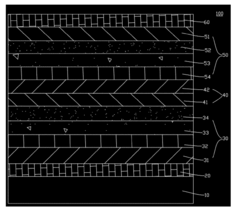
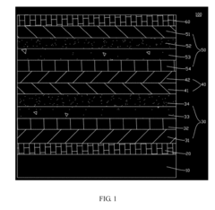
QNED Manufacturing Process
The QNED (Quantum Nano Emitting Diode) manufacturing process represents a significant advancement in display technology, combining the benefits of quantum dots and mini-LED backlighting. This process involves several intricate steps to achieve the high-performance display characteristics associated with QNED technology.
The foundation of QNED manufacturing lies in the production of quantum dots, typically composed of semiconductor nanocrystals. These quantum dots are synthesized through precise chemical processes, controlling their size and composition to achieve specific light emission properties. The quantum dots are then integrated into a film or layer that will serve as the color conversion element in the display.
Concurrently, the mini-LED backlight units are manufactured. This process involves the production of extremely small LED chips, typically measuring less than 200 micrometers. These mini-LEDs are fabricated using advanced semiconductor manufacturing techniques, including epitaxial growth, photolithography, and etching processes. The mini-LEDs are then precisely placed on a substrate using high-precision pick-and-place equipment.
The integration of the quantum dot layer with the mini-LED backlight is a critical step in QNED manufacturing. This process requires careful alignment and bonding to ensure optimal light transmission and color conversion. Advanced optical bonding techniques are employed to minimize light loss and maintain the integrity of the quantum dot layer.
To complete the QNED panel, additional layers such as light guide plates, diffusers, and polarizers are incorporated. These components work in concert to enhance light distribution, improve viewing angles, and optimize overall display performance. The assembly process demands stringent quality control measures to maintain consistency across the entire display surface.
Finally, the QNED panel undergoes extensive testing and calibration. This includes color accuracy verification, uniformity checks, and performance evaluations under various lighting conditions. Advanced imaging equipment and spectrophotometers are utilized to ensure that each QNED display meets the rigorous standards for color gamut, brightness, and contrast.
The QNED manufacturing process represents a convergence of multiple advanced technologies, requiring expertise in quantum dot synthesis, LED fabrication, and precision assembly. As the technology continues to evolve, manufacturers are focusing on improving yield rates, reducing production costs, and scaling up for mass production to make QNED displays more accessible to a broader market.
Unlock deeper insights with Patsnap Eureka Quick Research — get a full tech report to explore trends and direct your research. Try now!
Generate Your Research Report Instantly with AI Agent
Supercharge your innovation with Patsnap Eureka AI Agent Platform!