QNED: Advancements in Display Pixel Efficiency
JUN 19, 20259 MIN READ
Generate Your Research Report Instantly with AI Agent
Patsnap Eureka helps you evaluate technical feasibility & market potential.
QNED Technology Evolution
QNED (Quantum Nano Emitting Diode) technology has undergone significant evolution since its inception, marking a revolutionary advancement in display pixel efficiency. The journey of QNED began with the fundamental research into quantum dot materials and their potential application in display technologies.
In the early stages, researchers focused on developing stable quantum dot materials that could emit light efficiently when excited. This phase involved extensive experimentation with various semiconductor nanocrystals, particularly those based on cadmium selenide (CdSe) and indium phosphide (InP). The primary challenge was to create quantum dots with precise size control and uniform distribution, as these factors directly influence the color purity and efficiency of light emission.
As the understanding of quantum dot behavior improved, the next phase of QNED evolution centered on integrating these nanoparticles into display structures. This involved developing new manufacturing processes to deposit quantum dots onto substrates and create functional pixel arrays. Researchers explored various deposition techniques, including inkjet printing and photolithography, to achieve high-resolution displays with quantum dot emitters.
A significant milestone in QNED technology was the development of blue light-emitting diodes (LEDs) as the excitation source for quantum dots. This breakthrough allowed for a more efficient energy transfer mechanism, where blue light from the LED excites the quantum dots to emit red and green light, resulting in a full-color display. The combination of blue LEDs and quantum dots marked a turning point in display efficiency, as it eliminated the need for color filters that typically reduce brightness in traditional LCD displays.
Further advancements focused on improving the stability and longevity of quantum dot materials. Early QNED prototypes faced challenges related to degradation under high-energy blue light exposure and environmental factors. Researchers developed encapsulation techniques and protective layers to shield quantum dots from oxygen and moisture, significantly enhancing their operational lifespan.
Recent years have seen a shift towards environmentally friendly quantum dot materials, addressing concerns about the toxicity of cadmium-based compounds. This has led to the development of indium-based quantum dots and other heavy metal-free alternatives, which maintain high efficiency while complying with stringent environmental regulations.
The latest phase of QNED evolution has focused on scaling up production and improving manufacturing yields. This includes refining processes for large-area deposition of quantum dots and developing quality control measures to ensure consistent performance across large displays. Additionally, researchers are exploring new quantum dot architectures, such as perovskite quantum dots, which promise even higher efficiency and color purity.
As QNED technology continues to mature, ongoing research is aimed at further enhancing pixel efficiency, reducing power consumption, and expanding the color gamut. The evolution of QNED represents a convergence of nanotechnology, materials science, and display engineering, promising to revolutionize the visual quality and energy efficiency of next-generation displays.
Market Demand Analysis
The market demand for QNED (Quantum Nano Emitting Diode) technology in display pixel efficiency is experiencing significant growth, driven by the increasing consumer appetite for high-quality, energy-efficient displays across various sectors. As consumers become more discerning about display quality, there is a growing demand for technologies that can deliver superior color accuracy, brightness, and contrast while maintaining energy efficiency.
In the consumer electronics market, QNED displays are gaining traction, particularly in high-end televisions and monitors. The technology's ability to provide enhanced color volume and improved HDR performance is attracting consumers who seek immersive viewing experiences. This demand is further fueled by the rising popularity of 4K and 8K content, which requires displays capable of rendering fine details and vibrant colors accurately.
The automotive industry is another key driver of QNED market demand. As vehicles become more technologically advanced, there is an increasing need for high-quality, durable displays for infotainment systems, digital dashboards, and heads-up displays. QNED technology's potential to offer superior visibility in various lighting conditions, including bright sunlight, makes it particularly attractive for automotive applications.
In the professional and commercial display sector, QNED is garnering interest for its potential in digital signage, control rooms, and medical imaging. The technology's ability to deliver high brightness and color accuracy while maintaining energy efficiency is crucial in these applications where displays often operate for extended periods.
The gaming industry is also contributing to the market demand for QNED displays. Gamers are constantly seeking displays with faster response times, higher refresh rates, and better color reproduction. QNED technology's potential to meet these requirements while offering improved energy efficiency is likely to drive adoption in gaming monitors and high-end gaming laptops.
As remote work and virtual collaboration continue to be prevalent, there is an increased demand for high-quality displays in home office setups. QNED's potential to reduce eye strain through improved brightness control and color accuracy is attracting consumers who spend long hours in front of screens.
The market for QNED technology is also being influenced by broader trends in sustainability and energy efficiency. As governments and organizations worldwide implement stricter energy regulations, there is a growing demand for display technologies that can deliver high performance while minimizing power consumption. QNED's potential to offer improved efficiency compared to traditional LED and OLED technologies positions it favorably in this context.
QNED Technical Challenges
QNED (Quantum Nano Emitting Diode) technology, while promising significant advancements in display pixel efficiency, faces several technical challenges that need to be addressed for widespread adoption and commercialization. One of the primary hurdles is the complexity of manufacturing processes required to produce QNED displays at scale. The precise placement and alignment of quantum dots and nanoparticles demand highly sophisticated and controlled production environments, which can be difficult to achieve consistently in large-scale manufacturing.
Another significant challenge lies in the stability and longevity of QNED pixels. Quantum dots are known to be sensitive to environmental factors such as heat, moisture, and oxygen exposure. Ensuring the long-term stability of these nanostructures within the display matrix is crucial for maintaining consistent color output and overall display performance over time. This necessitates the development of robust encapsulation techniques and protective layers to shield the quantum dots from degradation.
Color accuracy and uniformity present additional technical hurdles. While QNED technology promises superior color reproduction, achieving precise control over the emission spectra of quantum dots across the entire display area remains challenging. Variations in quantum dot size and composition can lead to inconsistencies in color output, requiring advanced quality control measures and potentially complex calibration processes to ensure uniform visual performance across the display.
Power efficiency, although improved compared to traditional LED displays, still poses challenges for QNED technology. Optimizing the energy transfer from the blue micro-LED backlight to the quantum dots, while minimizing losses and maximizing light output, requires careful engineering of materials and structures. Balancing power consumption with brightness and color performance is an ongoing area of research and development.
The integration of QNED technology with existing display manufacturing infrastructure presents another set of challenges. Adapting current production lines and equipment to accommodate the unique requirements of QNED displays may require significant investments and retooling. This transition could potentially slow down the adoption of QNED technology in the short term, as manufacturers weigh the costs and benefits of upgrading their facilities.
Lastly, the cost of materials and production remains a significant barrier to widespread QNED adoption. The use of rare earth elements in quantum dots and the complex manufacturing processes contribute to higher production costs compared to conventional display technologies. Developing more cost-effective materials and streamlining production methods are crucial for making QNED displays economically viable for mass-market applications.
Current QNED Solutions
01 Quantum dot-based light emitting diodes for improved efficiency
QNED displays utilize quantum dot-based light emitting diodes to enhance pixel efficiency. These nanoscale semiconductor structures offer superior color purity, brightness, and energy efficiency compared to traditional display technologies. The quantum confinement effect in these nanostructures allows for precise control over emission wavelengths, resulting in improved color gamut and overall display performance.- Quantum dot structure for improved efficiency: QNED displays utilize quantum dot structures to enhance pixel efficiency. These structures are designed to improve light emission and color purity, resulting in better overall display performance. The quantum dots are typically embedded in a matrix or arranged in specific patterns to optimize their light-emitting properties.
- Nano-emitting diode architecture: The architecture of nano-emitting diodes in QNED displays is crucial for pixel efficiency. This includes the design of the diode structure, electrode configuration, and the integration of quantum dots. Advanced fabrication techniques are employed to create nanoscale structures that maximize light output and minimize energy loss.
- Color conversion and light management: QNED displays employ sophisticated color conversion techniques and light management strategies to enhance pixel efficiency. This involves the use of color filters, wavelength conversion layers, and optical structures to optimize light extraction and color reproduction. These techniques help to improve the overall brightness and color gamut of the display.
- Driving and control methods for QNED pixels: Efficient driving and control methods are essential for maximizing the performance of QNED display pixels. This includes advanced driving circuits, voltage control techniques, and timing algorithms that optimize the operation of quantum nano-emitting diodes. These methods help to reduce power consumption while maintaining high image quality.
- Integration with other display technologies: QNED technology can be integrated with other display technologies to further enhance pixel efficiency. This may involve combining QNED elements with OLED or LCD components, or incorporating advanced backplane technologies. Such hybrid approaches can leverage the strengths of multiple technologies to achieve superior display performance.
02 Nanostructure design for enhanced light extraction
Optimizing the nanostructure design of QNED pixels can significantly improve light extraction efficiency. This includes engineering the shape, size, and arrangement of quantum dots, as well as incorporating photonic crystal structures or plasmonic elements. These enhancements can reduce internal reflection and increase the amount of light emitted from the device, thereby improving overall pixel efficiency.Expand Specific Solutions03 Integration of quantum dots with micro-LED technology
Combining quantum dots with micro-LED technology in QNED displays can lead to significant improvements in pixel efficiency. This hybrid approach leverages the high brightness and fast response times of micro-LEDs with the superior color performance of quantum dots. The integration can be achieved through various methods, such as color conversion layers or direct quantum dot deposition on micro-LED structures.Expand Specific Solutions04 Advanced materials and fabrication techniques
Developing advanced materials and fabrication techniques is crucial for enhancing QNED pixel efficiency. This includes exploring new quantum dot compositions, improving quantum yield, and optimizing the charge transport layers. Novel deposition methods, such as inkjet printing or lithographic techniques, can enable precise control over quantum dot placement and density, leading to more efficient and uniform pixel performance.Expand Specific Solutions05 Driving and control circuitry optimization
Optimizing the driving and control circuitry for QNED displays can significantly impact pixel efficiency. This involves developing advanced thin-film transistor (TFT) backplanes, implementing sophisticated voltage and current control schemes, and integrating compensation algorithms to ensure uniform brightness and color across the display. Efficient power management and reduced parasitic capacitances can further enhance overall display performance.Expand Specific Solutions
Key QNED Industry Players
The QNED (Quantum Nano Emitting Diode) display technology market is in its early growth stage, with major players like Samsung Display, LG Display, and BOE Technology Group leading the development. The market size is expanding rapidly, driven by increasing demand for high-quality, energy-efficient displays in various applications. Technologically, QNED is still evolving, with companies like Sony, Sharp, and Japan Display actively researching and patenting advancements in pixel efficiency. While not yet fully mature, QNED shows promise in bridging the gap between QLED and OLED technologies, with key players like Samsung and LG pushing for commercialization in the near future.
Samsung Display Co., Ltd.
Technical Solution: Samsung Display has developed QNED (Quantum Nano Emitting Diode) technology, which combines quantum dot color conversion with nanorod LED light sources. This approach uses ultra-small nanorod LEDs as the light source, with each pixel composed of red, green, and blue nanorods. The quantum dots are then used to enhance color purity and efficiency. Samsung's QNED displays aim to achieve higher brightness, improved color volume, and better energy efficiency compared to traditional LCD and OLED technologies.
Strengths: Superior color accuracy and wider color gamut due to quantum dot technology. Potential for higher peak brightness than OLED. Improved energy efficiency. Weaknesses: Complex manufacturing process may lead to higher initial costs. Potential for differential aging of different color nanorods.
BOE Technology Group Co., Ltd.
Technical Solution: BOE has been working on QNED technology as part of its next-generation display development. Their approach focuses on integrating quantum dot color conversion layers with miniLED backlighting to create a hybrid QNED display. This technology aims to combine the high contrast ratio of miniLED with the wide color gamut of quantum dots. BOE's QNED displays are designed to offer improved HDR performance, enhanced color accuracy, and increased energy efficiency compared to traditional LCD panels.
Strengths: Potential for high brightness and excellent HDR performance. Improved color accuracy and wider color gamut. Leverages existing manufacturing infrastructure. Weaknesses: May not achieve the perfect blacks of OLED technology. Complexity in precisely controlling miniLED local dimming zones.
QNED Core Innovations
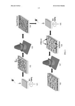
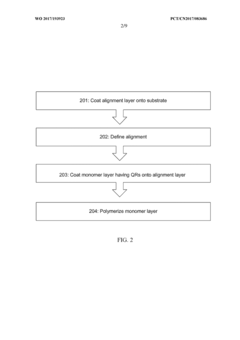
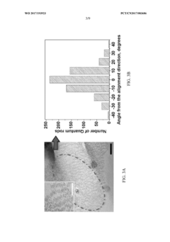
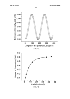
Photoaligned quantum rod enhancement films
PatentWO2017193923A1
Innovation
- Utilization of photoalignment technique to align quantum rods in a polymer layer, enabling precise control over local orientation.
- Integration of quantum rod enhancement film (QREF) into LCD displays to improve optical efficiency and color gamut without significant light loss.
- Development of a scalable production method for QREF, involving photoalignment layer coating, alignment, and subsequent polymerization of quantum rod-containing monomer layer.
Layered light-emitting structure with roughened interface
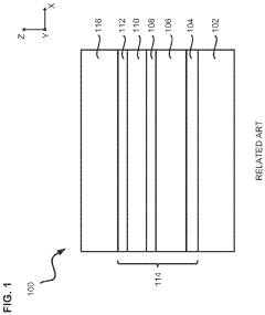
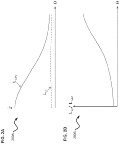
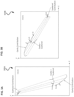
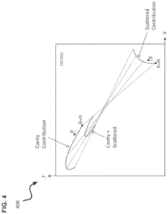
PatentActiveUS20220399526A1
Innovation
- Introducing a controlled interface roughness between layers of the light-emitting structure, specifically with a root mean square roughness between 5 nm and 30 nm, to create a scattering component that complements the cavity component, thereby reducing angular color shifts and maintaining luminance with varying viewing angles.
QNED Energy Efficiency
QNED (Quantum Nano Emitting Diode) technology represents a significant advancement in display pixel efficiency, particularly in terms of energy consumption. This innovative display technology combines the benefits of quantum dots and mini-LED backlighting to achieve superior color accuracy, brightness, and power efficiency compared to traditional LCD and OLED displays.
The energy efficiency of QNED displays is primarily attributed to their unique pixel structure and light emission mechanism. Unlike conventional LCDs that rely on color filters to produce different hues, QNED utilizes quantum dots to directly emit light of specific wavelengths. This approach eliminates the need for color filters, which typically absorb a significant portion of the backlight, resulting in improved energy efficiency.
Furthermore, QNED displays employ mini-LED backlighting, which allows for more precise local dimming control. This feature enables the display to selectively illuminate only the required areas of the screen, reducing power consumption in darker scenes. The combination of quantum dots and mini-LEDs also contributes to higher peak brightness levels while maintaining lower overall power consumption compared to OLED displays.
The nano-scale size of quantum dots in QNED displays plays a crucial role in their energy efficiency. These tiny semiconductor particles exhibit excellent light-emitting properties and can be tuned to produce specific colors with high purity. This precision in color reproduction allows QNED displays to achieve a wider color gamut while consuming less power than traditional display technologies.
Another factor contributing to QNED's energy efficiency is its improved thermal management. The use of mini-LEDs as a backlight source generates less heat compared to traditional LED backlighting systems. This reduced heat generation not only improves the overall energy efficiency but also enhances the longevity of the display panel.
The energy-saving potential of QNED technology extends beyond the display itself. By providing higher brightness and contrast ratios at lower power consumption levels, QNED displays can potentially reduce the overall energy requirements of devices such as televisions, monitors, and mobile devices. This efficiency gain becomes particularly significant in large-format displays, where power consumption is a critical factor.
As QNED technology continues to evolve, researchers and manufacturers are focusing on further improving its energy efficiency. Ongoing developments include optimizing quantum dot materials for even higher light conversion efficiency, refining mini-LED backlighting systems for more precise control, and developing advanced power management algorithms to maximize energy savings across various usage scenarios.
QNED Manufacturing Process
The QNED (Quantum Nano Emitting Diode) manufacturing process represents a significant advancement in display technology, combining the benefits of quantum dot and mini-LED technologies. This process involves several key steps that contribute to the enhanced pixel efficiency and overall display performance.
The first stage of QNED manufacturing focuses on the preparation of quantum dot materials. These nanocrystals are synthesized using precise chemical processes to achieve specific sizes and compositions, which determine the color and efficiency of light emission. The quantum dots are then carefully dispersed in a suitable matrix material to ensure uniform distribution and prevent aggregation.
Next, the mini-LED backlight units are fabricated. This involves the production of ultra-small LED chips, typically measuring less than 200 micrometers in size. These mini-LEDs are manufactured using advanced semiconductor processes, including epitaxial growth, photolithography, and etching techniques. The miniaturization of LEDs allows for a higher density of light sources, contributing to improved local dimming capabilities and contrast ratios.
The integration of quantum dots with mini-LEDs is a critical step in the QNED manufacturing process. This is achieved through various methods, such as on-chip integration or remote phosphor configurations. In on-chip integration, quantum dots are directly applied to the mini-LED surface, while remote phosphor configurations involve placing a quantum dot layer at a distance from the LED array.
The assembly of the QNED panel involves precise alignment and bonding of multiple layers. This includes the mini-LED backlight unit, quantum dot layer, LCD panel, and other optical components. Advanced automation and robotics are employed to ensure accurate placement and minimize manufacturing defects.
Quality control is a crucial aspect of the QNED manufacturing process. Rigorous testing procedures are implemented at various stages to verify the performance and uniformity of the display. This includes color calibration, brightness measurements, and defect detection using high-resolution imaging systems.
Finally, the QNED panels undergo encapsulation and packaging processes to protect the sensitive components from environmental factors and ensure long-term reliability. This may involve the use of specialized barrier films and sealants to prevent moisture ingress and maintain the stability of the quantum dot materials.
The QNED manufacturing process continues to evolve as researchers and engineers explore new techniques to enhance efficiency and reduce production costs. Ongoing developments include the optimization of quantum dot synthesis, improvements in mini-LED fabrication, and the exploration of novel integration methods to further boost display performance and energy efficiency.
Unlock deeper insights with Patsnap Eureka Quick Research — get a full tech report to explore trends and direct your research. Try now!
Generate Your Research Report Instantly with AI Agent
Supercharge your innovation with Patsnap Eureka AI Agent Platform!