QNED: Next-Level Display Resolution and Clarity
JUN 19, 20259 MIN READ
Generate Your Research Report Instantly with AI Agent
Patsnap Eureka helps you evaluate technical feasibility & market potential.
QNED Technology Overview
QNED (Quantum Nano Emitting Diode) technology represents a significant leap forward in display technology, combining the best aspects of QLED and OLED displays. This innovative approach utilizes quantum dots and mini-LEDs to create a display that offers superior brightness, contrast, and color accuracy compared to existing technologies.
At its core, QNED technology employs a matrix of mini-LEDs as the backlight source. These mini-LEDs are significantly smaller than traditional LED backlights, allowing for more precise local dimming and improved contrast ratios. The mini-LEDs are coupled with quantum dots, nano-scale semiconductor particles that emit light of specific wavelengths when excited by an energy source.
The quantum dots in QNED displays are responsible for producing the vibrant colors viewers see on screen. When the mini-LED backlight excites these quantum dots, they emit light at specific wavelengths corresponding to red, green, and blue colors. This process results in a wider color gamut and more accurate color reproduction compared to traditional LCD displays.
One of the key advantages of QNED technology is its ability to achieve deep blacks and high contrast ratios. The mini-LED backlight can be dimmed or turned off in specific areas of the screen, creating true blacks in dark scenes while maintaining brightness in lighter areas. This local dimming capability allows QNED displays to approach the contrast levels of OLED screens while offering higher peak brightness.
QNED displays also boast improved energy efficiency compared to traditional LED-LCD screens. The combination of mini-LEDs and quantum dots allows for more efficient light production and color conversion, resulting in lower power consumption without sacrificing picture quality.
In terms of durability and longevity, QNED technology offers advantages over OLED displays. Unlike OLED panels, which can suffer from burn-in issues over time, QNED screens are less susceptible to this problem due to their use of inorganic materials in the quantum dots and mini-LEDs.
The implementation of QNED technology promises to deliver next-level display resolution and clarity. By combining the high brightness capabilities of LED technology with the color accuracy and contrast of quantum dots, QNED displays can offer HDR performance that surpasses both QLED and OLED technologies in many aspects.
As QNED technology continues to evolve, we can expect to see further improvements in areas such as color volume, viewing angles, and response times. These advancements will likely position QNED as a strong contender in the high-end display market, offering consumers and professionals alike a compelling option for premium visual experiences.
Market Demand Analysis
The market demand for QNED (Quantum Nano Emitting Diode) technology is rapidly growing as consumers and industries seek superior display solutions with enhanced resolution and clarity. This emerging technology combines the benefits of quantum dots and mini-LED backlighting, positioning itself as a potential game-changer in the display market.
Consumer electronics, particularly high-end televisions and monitors, represent the primary market segment driving QNED demand. As 4K and 8K content becomes more prevalent, there is an increasing need for displays capable of rendering these ultra-high-resolution images with exceptional clarity and color accuracy. QNED technology addresses this demand by offering improved contrast ratios, wider color gamuts, and enhanced brightness levels compared to traditional LCD and OLED displays.
The professional and commercial sectors also contribute significantly to QNED market demand. Industries such as graphic design, video production, and digital signage require displays with superior color reproduction and image quality. QNED's ability to deliver vibrant, true-to-life colors and deep blacks makes it an attractive option for these applications.
Market research indicates a growing consumer willingness to invest in premium display technologies. As awareness of QNED's benefits increases, it is expected to capture a larger share of the high-end display market. The technology's potential to offer OLED-like picture quality at a more competitive price point is likely to accelerate its adoption in mid-range consumer electronics as well.
The automotive industry presents another promising market for QNED technology. As vehicles become more technologically advanced, there is a rising demand for high-quality in-car displays for infotainment systems, digital dashboards, and rear-seat entertainment. QNED's superior brightness and contrast characteristics make it well-suited for automotive applications, where displays must perform well in varying lighting conditions.
Global market trends suggest a shift towards larger screen sizes in both residential and commercial settings. QNED technology is well-positioned to capitalize on this trend, as it can maintain image quality and energy efficiency across larger display areas more effectively than some competing technologies.
The ongoing transition to 5G networks and the increasing popularity of streaming services are driving demand for displays capable of showcasing high-quality content. As content creators and distributors invest in higher resolution and HDR formats, there is a corresponding need for display technologies that can fully realize these advancements. QNED's ability to deliver enhanced contrast and color accuracy aligns well with these market requirements.
In conclusion, the market demand for QNED technology is robust and multifaceted, spanning consumer electronics, professional applications, and emerging sectors like automotive displays. As the technology matures and production scales up, it is expected to play a significant role in shaping the future of display markets, offering a compelling balance of performance and cost-effectiveness.
QNED Technical Challenges
QNED (Quantum Nano Emitting Diode) technology, while promising significant advancements in display resolution and clarity, faces several technical challenges that need to be addressed for widespread adoption and commercialization.
One of the primary challenges is the precise control and uniformity of quantum dot size and distribution. The size of quantum dots directly affects the color and brightness of emitted light, making uniformity crucial for consistent image quality. Achieving this level of precision at scale remains a significant hurdle, requiring advancements in manufacturing processes and quality control techniques.
Another major challenge lies in the development of efficient and stable blue QNED emitters. While red and green quantum dots have shown promising results, blue emitters tend to have lower efficiency and shorter lifespans. This imbalance can lead to color shift over time and reduced overall display performance. Researchers are exploring various materials and structures to improve blue QNED stability and efficiency.
The integration of QNED technology with existing display architectures presents another set of challenges. Adapting current manufacturing processes and equipment to accommodate QNED production requires significant investment and innovation. This includes developing new deposition techniques, patterning methods, and encapsulation technologies to protect the sensitive quantum dot layers.
Heat management is a critical issue in QNED displays. Quantum dots are sensitive to temperature fluctuations, which can affect their emission properties and longevity. Developing effective thermal management solutions that can dissipate heat without compromising display performance or increasing device thickness is essential.
Addressing the environmental and health concerns associated with certain quantum dot materials is another challenge. Some traditional quantum dot compositions contain heavy metals, raising concerns about toxicity and environmental impact. Research is ongoing to develop safer, cadmium-free alternatives that maintain high performance standards.
Scaling up production while maintaining cost-effectiveness is a significant hurdle for QNED technology. The current production processes for high-quality quantum dots are complex and expensive, potentially limiting their adoption in mass-market consumer electronics. Developing more efficient and economical manufacturing methods is crucial for the commercial viability of QNED displays.
Lastly, optimizing the driving circuits and algorithms for QNED displays presents unique challenges. The specific characteristics of quantum dot emitters require tailored approaches to color management, brightness control, and power efficiency. This necessitates the development of specialized hardware and software solutions to fully leverage the potential of QNED technology.
Current QNED Solutions
01 Quantum dot structure for enhanced light emission
QNED displays utilize advanced quantum dot structures to enhance light emission efficiency and color purity. These structures often incorporate multiple layers or shells to improve quantum confinement and reduce defects, resulting in higher resolution and clarity.- Quantum dot structure for enhanced light emission: QNED displays utilize advanced quantum dot structures to enhance light emission efficiency and color purity. These structures often incorporate multiple layers of semiconductor materials and precise control of quantum dot size and composition to optimize light output and spectral characteristics, resulting in improved display resolution and clarity.
- Nano-scale light-emitting diode design: QNED displays employ nano-scale light-emitting diodes that are engineered to achieve high brightness and efficiency. The design of these nano-LEDs often involves innovative electrode configurations, current spreading layers, and quantum well structures to maximize light output and minimize power consumption, contributing to enhanced display performance.
- Color conversion and light management techniques: To improve resolution and clarity, QNED displays incorporate advanced color conversion and light management techniques. These may include the use of color filters, quantum dot color converters, and micro-lens arrays to enhance color gamut, reduce light loss, and improve overall image quality.
- Pixel architecture and driving methods: QNED displays feature innovative pixel architectures and driving methods to achieve high resolution and clarity. This includes the development of sub-pixel arrangements, active matrix backplanes, and advanced driving schemes that enable precise control of individual nano-LEDs, resulting in improved image sharpness and reduced motion blur.
- Integration of quantum dots with micro-LED technology: QNED displays often combine quantum dot technology with micro-LED architecture to achieve superior resolution and clarity. This integration involves precise deposition of quantum dots onto micro-LED arrays, optimization of energy transfer between the two components, and development of manufacturing processes that ensure uniform and stable performance across the display.
02 Nano-scale emitting diodes for improved pixel density
QNED displays employ nano-scale emitting diodes, which allow for higher pixel density and improved resolution. The small size of these diodes enables more precise control over light emission and reduces crosstalk between pixels, enhancing overall image clarity.Expand Specific Solutions03 Advanced materials and fabrication techniques
The development of QNED displays involves the use of advanced materials and fabrication techniques to achieve high-resolution and clear displays. This includes the integration of novel semiconductor materials, precise deposition methods, and innovative patterning techniques to create uniform and efficient light-emitting structures.Expand Specific Solutions04 Optimization of display backplane and driving circuits
QNED displays incorporate optimized backplane designs and driving circuits to support high-resolution imaging. This includes the development of thin-film transistor (TFT) arrays with improved electron mobility and advanced addressing schemes to enable precise control of individual pixels, enhancing overall display clarity.Expand Specific Solutions05 Color management and image processing techniques
To maximize the resolution and clarity of QNED displays, advanced color management and image processing techniques are employed. These include algorithms for color calibration, contrast enhancement, and motion compensation, which work in conjunction with the quantum nano-emitting diodes to produce sharp, vibrant images with high fidelity.Expand Specific Solutions
Key QNED Industry Players
The QNED (Quantum Nano Emitting Diode) display technology market is in its early growth stage, with significant potential for expansion. The global market size for advanced display technologies is projected to reach billions of dollars in the coming years. QNED technology is still evolving, with varying levels of maturity among key players. Companies like Samsung Electronics and LG Display are at the forefront, leveraging their expertise in quantum dot and mini-LED technologies. BOE Technology Group and Semiconductor Energy Laboratory are also making strides in QNED research. Other players like Huawei Technologies and Xiaomi are exploring QNED applications for mobile devices. The competitive landscape is dynamic, with both established display manufacturers and emerging tech companies vying for market share in this promising field.
BOE Technology Group Co., Ltd.
Technical Solution: BOE has been actively researching and developing QNED technology as part of its next-generation display solutions. Their approach focuses on integrating quantum dot color conversion layers with micro-LED backlights to achieve superior color performance and brightness. BOE's QNED displays aim to offer higher contrast ratios, wider color gamut, and improved energy efficiency compared to conventional LCD and OLED technologies. The company is working on scaling up the production of QNED displays for various applications, including high-end TVs, monitors, and automotive displays.
Strengths: Strong expertise in display manufacturing, potential for cost-effective production at scale. Weaknesses: Relatively new to QNED technology, may face challenges in competing with more established players in the field.
Samsung Electronics Co., Ltd.
Technical Solution: Samsung has developed QNED (Quantum Nano Emitting Diode) technology, which combines quantum dot and micro-LED technologies. This hybrid approach uses ultra-small LEDs as the light source, with a layer of quantum dots for color conversion. The result is a display with superior brightness, contrast, and color accuracy compared to traditional LCD or OLED displays. Samsung's QNED displays can achieve higher pixel densities and better energy efficiency, potentially revolutionizing next-level display resolution and clarity.
Strengths: Exceptional brightness and contrast, wide color gamut, improved energy efficiency, and potential for higher pixel densities. Weaknesses: Complex manufacturing process, potentially high production costs in the initial stages.
QNED Core Innovations
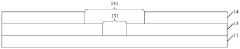
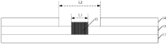
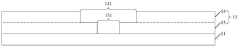
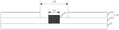
Display panel and display device
PatentActiveCN113488500B
Innovation
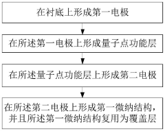
- Design a display panel that ensures that by setting a first opening on the first pixel definition layer that matches the size of the light-emitting unit, and setting a second opening on the second pixel definition layer with a minimum width greater than or equal to the maximum length of the light-emitting unit. The light-emitting unit can perform all-round rotation and alignment in the second opening to avoid random drift and ensure that the light-emitting unit falls back into the corresponding first opening.
QLED device, display device and manufacturing method
PatentPendingCN115472762A
Innovation
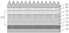
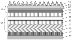
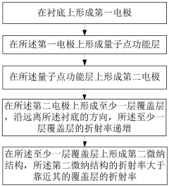
- A micro-nano structure formed by ferroelectric materials is introduced into the QLED device. The refractive index of the micro-nano structure is greater than the refractive index of the second electrode, which is used to change the incident angle of the light emitted from the quantum dot functional layer at the exit interface, and increases through the refractive index. The overlay design increases the critical angle, thereby improving light extraction efficiency.
QNED Manufacturing Process
The QNED (Quantum Nano Emitting Diode) manufacturing process represents a significant advancement in display technology, combining the strengths of quantum dot and mini-LED technologies. This process involves several intricate steps, each crucial for achieving the superior image quality and performance associated with QNED displays.
The foundation of QNED manufacturing lies in the production of quantum dots, typically composed of semiconductor nanocrystals. These quantum dots are synthesized through precise chemical processes, controlling their size and composition to achieve specific light emission properties. The uniformity and quality of these quantum dots are paramount, as they directly influence the color accuracy and brightness of the final display.
Once the quantum dots are prepared, they are integrated into a film structure. This film serves as the color conversion layer, transforming the blue light from mini-LEDs into the desired red and green colors. The application of this quantum dot film requires extreme precision to ensure even distribution and optimal performance across the entire display surface.
The mini-LED backlight system forms another critical component of the QNED manufacturing process. These miniaturized LEDs are produced using advanced semiconductor fabrication techniques, often involving epitaxial growth processes. The mini-LEDs are then precisely arranged in an array, with each LED serving as an individual dimming zone, enabling superior local dimming capabilities.
The assembly of the QNED panel involves layering multiple components. The mini-LED backlight array is positioned behind the quantum dot film, followed by additional optical layers such as diffusers and polarizers. This layered structure is then integrated with the LCD panel, which modulates the light to create the final image.
A crucial aspect of QNED manufacturing is the implementation of advanced local dimming algorithms. These algorithms control the mini-LED backlight array, adjusting the brightness of individual zones to enhance contrast and reduce blooming effects. The development and fine-tuning of these algorithms are integral to maximizing the performance of QNED displays.
Quality control measures are rigorously applied throughout the manufacturing process. This includes testing for color accuracy, brightness uniformity, and contrast performance. Advanced imaging equipment and spectrophotometers are employed to ensure each QNED panel meets the stringent standards required for high-end display applications.
The QNED manufacturing process culminates in the final assembly and calibration of the display. This involves integrating the QNED panel with other components such as the display frame, electronics, and interfaces. Each display undergoes final adjustments and calibration to ensure optimal performance before being packaged for distribution.
QNED Energy Efficiency
QNED (Quantum Nano Emitting Diode) technology represents a significant advancement in display technology, offering superior image quality and brightness. However, energy efficiency remains a critical consideration in its development and adoption. QNED displays have shown promising results in terms of power consumption, potentially surpassing the efficiency of current OLED and LCD technologies.
The energy efficiency of QNED displays stems from their unique structure and operating principles. Unlike traditional LED displays, QNED utilizes quantum dots and nanorod LEDs, which can emit light more efficiently at lower power levels. This results in reduced energy consumption while maintaining high brightness and color accuracy.
One of the key factors contributing to QNED's energy efficiency is its ability to achieve high peak brightness with lower power input. This is particularly beneficial for HDR content, where high brightness is crucial for delivering a superior viewing experience. QNED displays can potentially reach peak brightness levels of up to 2,000 nits while consuming less power than comparable OLED or LCD panels.
The use of quantum dots in QNED technology also plays a significant role in enhancing energy efficiency. Quantum dots can convert blue light from the LED backlight into pure red and green light with minimal energy loss. This efficient color conversion process results in improved color accuracy and reduced power consumption compared to traditional color filter methods used in LCD displays.
Furthermore, QNED displays benefit from local dimming capabilities, allowing for precise control of backlight zones. This feature enables the display to selectively dim or turn off areas of the screen that don't require illumination, further reducing overall power consumption. The combination of efficient light emission and precise backlight control contributes to QNED's potential for superior energy efficiency.
Research and development efforts in QNED technology are focusing on further improving its energy efficiency. This includes optimizing the quantum dot and nanorod LED materials, enhancing the light extraction efficiency, and refining the backlight control algorithms. As the technology matures, it is expected that QNED displays will continue to push the boundaries of energy efficiency in high-performance display solutions.
The potential energy savings offered by QNED technology extend beyond individual devices. As large-format displays and video walls become increasingly prevalent in various industries, the adoption of energy-efficient QNED displays could lead to significant reductions in power consumption on a broader scale. This aligns with global efforts to reduce energy consumption and minimize the environmental impact of electronic devices.
Unlock deeper insights with Patsnap Eureka Quick Research — get a full tech report to explore trends and direct your research. Try now!
Generate Your Research Report Instantly with AI Agent
Supercharge your innovation with Patsnap Eureka AI Agent Platform!