Analysis of passivation film formation during electropolishing
OCT 11, 20259 MIN READ
Generate Your Research Report Instantly with AI Agent
Patsnap Eureka helps you evaluate technical feasibility & market potential.
Electropolishing Passivation Film Background and Objectives
Electropolishing, a critical surface finishing technique, has evolved significantly since its inception in the early 20th century. This electrochemical process selectively removes material from a metallic workpiece, resulting in improved surface finish, corrosion resistance, and aesthetic appeal. The formation of passivation films during electropolishing represents a fundamental aspect of this technology, governing both the process efficiency and the quality of the finished surface.
The historical development of electropolishing technology can be traced back to the 1930s when it was first applied to stainless steel components. Over subsequent decades, the technique has expanded to encompass a wide range of metals and alloys, including aluminum, copper, titanium, and various specialty alloys used in demanding industries such as aerospace, medical devices, and semiconductor manufacturing.
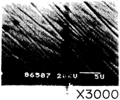
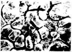
Recent technological advancements have shifted focus toward understanding and controlling the nanoscale mechanisms of passivation film formation during the electropolishing process. This microscopic layer, typically only a few nanometers thick, plays a crucial role in determining the final surface properties of the polished material. The composition, structure, and stability of these films vary significantly depending on the base material, electrolyte composition, and process parameters.
The primary objective of this technical research is to comprehensively analyze the formation mechanisms, characteristics, and influencing factors of passivation films during electropolishing across different metallic substrates. This includes investigating the electrochemical reactions at the metal-electrolyte interface, the kinetics of film growth, and the relationship between process parameters and film properties.
Current technological trends indicate a growing interest in developing more environmentally friendly electropolishing processes that maintain or enhance passivation film quality while reducing the use of hazardous chemicals. Additionally, there is significant momentum toward integrating real-time monitoring and control systems to optimize passivation film formation during the electropolishing process.
The ultimate goal of this research is to establish a fundamental understanding that enables precise control over passivation film characteristics, leading to enhanced surface properties tailored for specific applications. This knowledge will support the development of advanced electropolishing techniques capable of meeting increasingly stringent requirements in high-performance industries while addressing environmental and sustainability concerns.
The historical development of electropolishing technology can be traced back to the 1930s when it was first applied to stainless steel components. Over subsequent decades, the technique has expanded to encompass a wide range of metals and alloys, including aluminum, copper, titanium, and various specialty alloys used in demanding industries such as aerospace, medical devices, and semiconductor manufacturing.
Recent technological advancements have shifted focus toward understanding and controlling the nanoscale mechanisms of passivation film formation during the electropolishing process. This microscopic layer, typically only a few nanometers thick, plays a crucial role in determining the final surface properties of the polished material. The composition, structure, and stability of these films vary significantly depending on the base material, electrolyte composition, and process parameters.
The primary objective of this technical research is to comprehensively analyze the formation mechanisms, characteristics, and influencing factors of passivation films during electropolishing across different metallic substrates. This includes investigating the electrochemical reactions at the metal-electrolyte interface, the kinetics of film growth, and the relationship between process parameters and film properties.
Current technological trends indicate a growing interest in developing more environmentally friendly electropolishing processes that maintain or enhance passivation film quality while reducing the use of hazardous chemicals. Additionally, there is significant momentum toward integrating real-time monitoring and control systems to optimize passivation film formation during the electropolishing process.
The ultimate goal of this research is to establish a fundamental understanding that enables precise control over passivation film characteristics, leading to enhanced surface properties tailored for specific applications. This knowledge will support the development of advanced electropolishing techniques capable of meeting increasingly stringent requirements in high-performance industries while addressing environmental and sustainability concerns.
Market Applications and Industry Demand Analysis
The electropolishing market has witnessed substantial growth in recent years, driven primarily by increasing demand across multiple high-precision industries. The global electropolishing services market was valued at approximately $1.2 billion in 2022 and is projected to grow at a CAGR of 6.8% through 2030. This growth trajectory underscores the critical importance of understanding passivation film formation mechanisms to optimize electropolishing processes and meet evolving industry requirements.
Medical device manufacturing represents the largest application segment, accounting for nearly 35% of the total market share. The stringent regulatory requirements for surface finish in implantable devices, surgical instruments, and diagnostic equipment necessitate superior electropolishing techniques that produce consistent and predictable passivation films. The COVID-19 pandemic further accelerated demand in this sector, particularly for ventilator components and specialized medical equipment requiring contamination-free surfaces.
The semiconductor industry constitutes another significant market driver, where ultra-clean surfaces are essential for manufacturing microchips and electronic components. As chip architectures continue to shrink to nanometer scales, the quality of passivation films during electropolishing directly impacts device performance and reliability. Industry analysts predict this segment will experience the fastest growth rate at 8.2% annually through 2028.
Aerospace and defense applications have also emerged as key growth sectors, particularly for components used in aircraft engines, fuel systems, and satellite components. These applications demand electropolished surfaces with specific passivation characteristics to withstand extreme environmental conditions while maintaining structural integrity and corrosion resistance.
Pharmaceutical manufacturing equipment represents another significant market segment, where electropolished surfaces with controlled passivation films are essential for preventing product contamination and ensuring compliance with regulatory standards. The biopharmaceutical subsector, in particular, has shown increased demand for advanced electropolishing solutions that can maintain sterility in production environments.
Regionally, North America and Europe currently dominate the market with combined market share exceeding 60%, primarily due to their established medical device and aerospace industries. However, the Asia-Pacific region is experiencing the fastest growth rate, driven by rapid industrialization in China and India, alongside significant investments in semiconductor manufacturing facilities across Taiwan, South Korea, and Singapore.
Industry surveys indicate that manufacturers are increasingly prioritizing electropolishing processes that offer precise control over passivation film formation, as this directly correlates with product performance, longevity, and regulatory compliance. This trend has sparked renewed interest in advanced research focused on understanding and controlling the fundamental mechanisms of passivation film formation during electropolishing.
Current Challenges in Passivation Film Formation
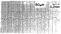
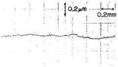
Despite significant advancements in electropolishing technology, the formation of passivation films during the process continues to present several critical challenges that impede optimal performance and reproducibility. One of the primary obstacles is the lack of real-time monitoring capabilities for passivation film formation. Current technologies struggle to provide accurate in-situ measurements of film thickness, composition, and uniformity during the electropolishing process, making it difficult to implement precise control mechanisms.
The complex interplay between electrolyte composition, current density, temperature, and material properties creates significant variability in passivation film characteristics. This multifactorial dependency makes standardization challenging across different material systems and geometries. Research indicates that even minor variations in process parameters can lead to substantial differences in film properties, affecting the final surface quality and performance.
Temporal stability of passivation films represents another significant challenge. Many passivation layers formed during electropolishing exhibit degradation over time, particularly when exposed to harsh environments or mechanical stresses. This degradation compromises the long-term protection provided by these films, necessitating additional post-processing steps or periodic maintenance.
The non-uniform distribution of current density across complex geometries results in inconsistent passivation film formation. Areas with high current density often experience accelerated dissolution and different passivation characteristics compared to low-current regions. This non-uniformity is particularly problematic for components with intricate shapes, internal features, or varying cross-sections.
Environmental and health concerns associated with traditional electropolishing electrolytes pose regulatory challenges. Many conventional formulations contain hazardous substances like chromic acid or hydrofluoric acid, which are facing increasing restrictions. Alternative, environmentally friendly electrolytes often fail to produce passivation films with comparable properties, creating a significant technological gap.
The fundamental mechanisms governing passivation film formation during electropolishing remain incompletely understood. The dynamic nature of the process, involving simultaneous dissolution and oxide formation, complicates theoretical modeling and prediction. This knowledge gap hinders the development of advanced control strategies and novel electrolyte formulations tailored for specific applications.
Scaling challenges persist when transitioning from laboratory-scale demonstrations to industrial implementation. Maintaining consistent passivation film properties across large surface areas or in high-volume production settings requires sophisticated engineering solutions that are not yet fully developed. These scaling issues often result in quality variations that are unacceptable for critical applications in medical, aerospace, or semiconductor industries.
Contemporary Methodologies for Passivation Film Analysis
01 Metal surface passivation techniques
Various techniques are employed for passivating metal surfaces to prevent corrosion and improve durability. These methods include chemical treatments, electrochemical processes, and the application of specialized coatings that form protective oxide layers. The passivation film acts as a barrier against environmental factors that could cause degradation of the metal substrate, extending the lifespan of components in various applications.- Metal surface passivation techniques: Various techniques are employed to form passivation films on metal surfaces to protect against corrosion and oxidation. These methods include chemical treatments, electrochemical processes, and thermal oxidation. The passivation layer acts as a protective barrier that prevents further reaction of the underlying metal with the environment, thereby enhancing durability and longevity of metal components.
- Semiconductor device passivation: Passivation films are critical in semiconductor manufacturing to protect electronic components from environmental factors and improve device reliability. These films typically consist of silicon dioxide, silicon nitride, or other dielectric materials that are deposited using techniques such as chemical vapor deposition (CVD) or atomic layer deposition (ALD). The passivation layer also serves to reduce surface states and improve electrical performance of semiconductor devices.
- Advanced passivation materials for solar cells: Novel materials and compositions are being developed for passivation films in photovoltaic applications to improve solar cell efficiency. These include aluminum oxide, hydrogenated amorphous silicon, and various metal oxides. The passivation layers reduce surface recombination of charge carriers and enhance light absorption, leading to higher conversion efficiencies in solar energy systems.
- Deposition methods for passivation films: Various deposition techniques are employed to form high-quality passivation films with precise thickness control and uniformity. These methods include plasma-enhanced chemical vapor deposition (PECVD), atomic layer deposition (ALD), sputtering, and solution-based processes. Each technique offers specific advantages in terms of film quality, process temperature, deposition rate, and compatibility with different substrate materials.
- Passivation for microelectromechanical systems (MEMS): Specialized passivation film formation techniques are developed for MEMS devices to protect moving parts and sensitive structures while maintaining functionality. These passivation approaches must address unique challenges such as conformal coverage of high-aspect-ratio structures, stress management, and compatibility with release processes. Materials like parylene, fluoropolymers, and self-assembled monolayers are often used to provide both electrical insulation and protection against environmental factors.
02 Semiconductor device passivation methods
Passivation films are critical in semiconductor manufacturing to protect electronic components from environmental contamination and mechanical damage. These films are typically formed using materials such as silicon nitride, silicon oxide, or polymeric compounds that provide electrical insulation and physical protection. Advanced deposition techniques ensure uniform coverage and optimal electrical properties of the passivation layer.Expand Specific Solutions03 Novel materials for passivation films
Research has led to the development of innovative materials for passivation films with enhanced properties. These include composite structures, nanoparticle-reinforced films, and organic-inorganic hybrid materials that offer superior barrier properties, flexibility, and durability. These advanced materials can be tailored to specific applications, providing improved protection against moisture, oxygen, and other contaminants.Expand Specific Solutions04 Deposition and formation processes
Various deposition techniques are employed for passivation film formation, including chemical vapor deposition (CVD), physical vapor deposition (PVD), atomic layer deposition (ALD), and solution-based methods. Process parameters such as temperature, pressure, and precursor chemistry significantly influence the quality and properties of the resulting films. Optimization of these parameters enables the creation of defect-free passivation layers with precise thickness control.Expand Specific Solutions05 Passivation for specific applications
Specialized passivation film technologies have been developed for specific applications such as solar cells, LEDs, MEMS devices, and battery components. These application-specific passivation solutions address unique challenges like high-temperature operation, exposure to harsh chemicals, or mechanical stress. The passivation films are engineered to enhance device performance while providing the necessary protection against environmental factors relevant to each application.Expand Specific Solutions
Leading Companies and Research Institutions in Electropolishing
Electropolishing passivation film formation technology is currently in a growth phase, with increasing applications in semiconductor, medical device, and electronics industries. The market is expanding at approximately 6-8% annually, driven by demand for high-precision surface finishing. Technologically, the field shows varying maturity levels across players. Industry leaders like Applied Materials and Samsung Electronics have developed advanced proprietary processes, while specialized firms such as Faraday Technology and Marui Galvanizing offer innovative niche solutions. Academic-industry collaborations involving Hunan University and Southern University of Science & Technology are accelerating fundamental research. The competitive landscape features both established semiconductor equipment manufacturers and specialized surface treatment companies, with increasing integration of electropolishing into broader manufacturing processes.
Applied Materials, Inc.
Technical Solution: Applied Materials has developed an advanced semiconductor wafer electropolishing system that precisely controls passivation film formation for critical semiconductor manufacturing applications. Their platform integrates real-time impedance spectroscopy to monitor the formation and evolution of the passivation layer during copper and other metal interconnect polishing. The system employs a proprietary electrolyte delivery mechanism that maintains optimal chemical gradients at the wafer surface, ensuring uniform passivation film development across 300mm wafers. Applied Materials' technology incorporates multi-zone process control with independently adjustable current densities across different wafer regions to compensate for edge effects and ensure uniform material removal. Their approach combines electrochemical modeling with machine learning algorithms that predict and control passivation film behavior based on wafer pattern density and feature geometry. This system has been particularly valuable for advanced node semiconductor manufacturing, where traditional chemical mechanical planarization (CMP) faces increasing challenges with pattern density effects and microscratching.
Strengths: Exceptional within-wafer uniformity control (<3% variation) through precise passivation film management. The process eliminates mechanical stress on fragile low-k dielectric structures common in advanced semiconductor nodes. Weaknesses: The system requires sophisticated facilities infrastructure including ultra-pure chemistry handling and precise temperature control. The technology demands significant process engineering expertise for recipe development and maintenance.
Faraday Technology, Inc.
Technical Solution: Faraday Technology has developed a proprietary Pulse/Pulse Reverse Electropolishing (PPREP) technology for passivation film formation during electropolishing. Their approach utilizes controlled current modulation with alternating anodic and cathodic pulses to precisely manage the formation and dissolution of the passivation layer. This technique allows for real-time control of the viscous salt film that forms at the metal-electrolyte interface, which is crucial for achieving uniform material removal and superior surface finish. The system incorporates advanced monitoring capabilities that analyze electrochemical impedance during the process to optimize pulse parameters based on workpiece geometry and material composition. Faraday's technology has demonstrated particular effectiveness for complex geometries and difficult-to-polish alloys like stainless steel, titanium, and nickel-based superalloys, where traditional DC electropolishing often produces inconsistent results.
Strengths: Superior control over passivation film dynamics, resulting in more uniform material removal even on complex geometries. The pulse technology reduces heat generation and prevents pitting defects common in conventional electropolishing. Weaknesses: Requires more sophisticated power supply equipment and process control systems than traditional methods, potentially increasing implementation costs. The technology may require material-specific parameter optimization for new alloy systems.
Critical Patents and Research on Passivation Mechanisms
Process for forming passive film on stainless steel, and stainless steel and gas- and liquid-contacting part
PatentWO1992021786A1
Innovation
- The method involves electropolishing the stainless steel surface, followed by high-temperature baking in an inert gas atmosphere, and then forming a passivated film by oxidizing the surface in an oxidizing gas atmosphere, with subsequent hydrogen treatment to reduce iron oxides and enhance the film's smoothness and corrosion resistance.
Nitinol Fatigue Resistance Using Electropolishing, Magnetoelectropolishing, Anodizing and Magnetoanodizing or Combinations Thereof Under Oxygen Evolution Regime
PatentInactiveUS20180291522A1
Innovation
- Performing electropolishing or magnetoelectropolishing processes under an oxygen evolution regime to increase oxygen adsorption, enrich the oxide layer, and reduce nickel content, thereby enhancing the material's fatigue resistance and surface homogeneity.
Environmental Impact and Sustainability Considerations
Electropolishing processes, while effective for surface finishing, present significant environmental considerations that must be addressed in modern industrial applications. The formation of passivation films during electropolishing typically involves chemical baths containing acids, heavy metals, and other potentially hazardous substances. These electrolytes, particularly those containing phosphoric and sulfuric acids, pose environmental risks if improperly managed. Waste streams from these processes contain dissolved metals, spent acids, and other contaminants that require specialized treatment before discharge to prevent water and soil contamination.
Recent advancements in electropolishing technology have focused on developing more environmentally friendly electrolyte formulations. Green chemistry approaches have yielded promising alternatives that reduce or eliminate chromium compounds and other toxic substances while maintaining effective passivation film formation. These eco-friendly electrolytes not only reduce environmental impact but also improve workplace safety by minimizing exposure to hazardous chemicals.
Energy consumption represents another significant environmental consideration in electropolishing operations. The electrical current required for the electrochemical reactions contributes to the carbon footprint of the process. Research indicates that optimizing current density and processing time can significantly reduce energy requirements while maintaining passivation film quality. Implementation of energy-efficient power supplies and process automation has demonstrated potential energy savings of 15-30% in industrial applications.
Water usage in electropolishing operations presents additional sustainability challenges. Traditional processes require substantial volumes for rinsing and cleaning stages. Closed-loop water recycling systems have emerged as effective solutions, reducing freshwater consumption by up to 80% in some facilities. Advanced filtration and ion exchange technologies enable the recovery and reuse of process water while maintaining the purity levels required for high-quality passivation film formation.
Life cycle assessment (LCA) studies of electropolishing processes reveal that the environmental impact extends beyond immediate operational concerns. The extraction and processing of raw materials for electrolytes, energy consumption during operation, and end-of-life management of spent solutions all contribute to the overall environmental footprint. Comprehensive sustainability approaches must therefore consider the entire value chain, from material sourcing to waste management.
Regulatory frameworks worldwide are increasingly addressing the environmental aspects of surface finishing technologies, including electropolishing. Compliance with standards such as REACH in Europe and similar regulations in other regions has driven innovation in more sustainable passivation techniques. Industries are now adopting integrated environmental management systems that monitor and minimize the ecological impact of electropolishing operations while ensuring effective passivation film formation.
Quality Standards and Compliance Requirements
Electropolishing processes must adhere to stringent quality standards and compliance requirements to ensure consistent passivation film formation and optimal surface properties. ASTM B912 specifically addresses the electropolishing of stainless steel, establishing parameters for surface finish, corrosion resistance, and passivation layer integrity. This standard requires that electropolished surfaces demonstrate a minimum chromium-to-iron ratio of 1.5:1 in the passive layer, which can be verified through X-ray photoelectron spectroscopy (XPS) analysis.
ISO 15730 provides comprehensive guidelines for electropolishing processes, including requirements for equipment calibration, solution maintenance, and quality control procedures. The standard emphasizes the importance of regular testing of the passivation film's thickness, uniformity, and chemical composition to ensure consistent performance across production batches.
For medical device applications, FDA 21 CFR Part 820 mandates strict quality management systems for electropolishing processes used in medical device manufacturing. These regulations require thorough documentation of process parameters, validation protocols, and regular testing to ensure that the passivation films formed during electropolishing meet biocompatibility requirements and maintain their integrity over the product lifecycle.
The semiconductor industry follows SEMI F19 standards, which establish specifications for electropolished surfaces in high-purity fluid handling components. These standards require extremely low particle generation and metal ion release from passivation films, with maximum allowable metal ion release rates typically below 10 parts per billion during standardized extraction tests.
Aerospace applications must comply with AMS 2700 specifications, which define acceptance criteria for electropolished surfaces on critical components. The standard requires that passivation films demonstrate resistance to salt spray testing per ASTM B117 for a minimum of 168 hours without showing signs of corrosion or degradation.
Environmental regulations, including EU RoHS and REACH, impact electropolishing processes by restricting the use of certain chemicals in polishing solutions. This has driven innovation in developing environmentally friendly electrolytes that can still produce high-quality passivation films while minimizing environmental impact and worker exposure to hazardous substances.
Quality control methods for passivation film assessment include electrochemical impedance spectroscopy (EIS), cyclic potentiodynamic polarization testing, and atomic force microscopy (AFM) for surface characterization. These techniques must be performed according to standardized protocols to ensure reliable and reproducible results that can be used to verify compliance with applicable standards.
Unlock deeper insights with Patsnap Eureka Quick Research — get a full tech report to explore trends and direct your research. Try now!
Generate Your Research Report Instantly with AI Agent
Supercharge your innovation with Patsnap Eureka AI Agent Platform!