Electropolishing for semiconductor and vacuum chamber applications
OCT 11, 202510 MIN READ
Generate Your Research Report Instantly with AI Agent
Patsnap Eureka helps you evaluate technical feasibility & market potential.
Electropolishing Technology Background and Objectives
Electropolishing emerged in the early 20th century as a surface finishing technique, but its application in semiconductor and vacuum chamber industries gained significant momentum only in the 1970s and 1980s. This electrochemical process selectively removes material from a metallic workpiece, resulting in smoothed surfaces with enhanced properties. The evolution of this technology has been closely tied to the increasing demands of high-purity environments required in semiconductor manufacturing and vacuum applications.
The semiconductor industry's rapid advancement has continuously pushed electropolishing technology to achieve higher precision and cleanliness standards. From the initial rudimentary applications, electropolishing has evolved to address micro and nano-scale surface requirements, particularly critical for ultra-high vacuum (UHV) systems and semiconductor processing equipment where even microscopic contaminants can cause catastrophic failures.
Current technological trends indicate a shift toward more environmentally friendly electropolishing solutions with reduced hazardous chemicals, while maintaining or improving performance characteristics. Additionally, there is growing interest in developing electropolishing techniques compatible with new alloys and composite materials increasingly used in advanced semiconductor fabrication equipment.
The primary objective of electropolishing in these applications is to achieve ultra-smooth surfaces with roughness values often below 10 nanometers Ra, which significantly reduces particle generation and outgassing in vacuum environments. Secondary objectives include enhanced corrosion resistance, improved cleanability, and extended component lifespan, all critical factors in semiconductor manufacturing where downtime is extremely costly.
Another key goal is the development of more precise control mechanisms for the electropolishing process, enabling consistent results across complex geometries and varying material compositions. This includes advanced monitoring systems that can provide real-time feedback during the electropolishing process, allowing for adjustments that optimize surface finish quality.
Research is also focused on understanding the fundamental electrochemical mechanisms at play during electropolishing, particularly at the micro and nano scales. This knowledge is essential for developing next-generation electropolishing technologies capable of meeting the increasingly stringent requirements of sub-5nm semiconductor nodes and quantum computing hardware.
The integration of electropolishing with other surface treatment technologies represents another important development direction, creating hybrid processes that combine the advantages of multiple techniques. These integrated approaches aim to address specific challenges in semiconductor and vacuum applications, such as hydrogen embrittlement prevention and enhanced particle removal efficiency.
Semiconductor and Vacuum Chamber Market Requirements
The semiconductor and vacuum chamber industries have witnessed exponential growth over the past decade, driven primarily by increasing demand for advanced electronic devices, cloud computing infrastructure, and emerging technologies such as artificial intelligence and Internet of Things. This growth has created stringent requirements for surface finishing technologies, particularly electropolishing, which plays a critical role in maintaining the integrity and performance of semiconductor manufacturing equipment and vacuum chambers.
In the semiconductor sector, market requirements for electropolishing have become increasingly demanding due to the continuous miniaturization of semiconductor devices. As node sizes shrink below 5nm, even microscopic surface imperfections can significantly impact yield rates and device performance. The global semiconductor equipment market, valued at approximately $103 billion in 2022, demands electropolishing solutions that can achieve surface roughness values below 0.1 μm Ra while maintaining dimensional accuracy within nanometer tolerances.
Vacuum chamber applications present equally rigorous requirements, particularly in high-energy physics research, aerospace, and semiconductor manufacturing environments. These chambers require ultra-high vacuum (UHV) conditions with pressures as low as 10^-12 Torr, necessitating surfaces with minimal outgassing characteristics and exceptional cleanliness. The global vacuum chamber market segment demands electropolishing processes that can effectively remove embedded contaminants and create oxide layers that minimize gas permeation and virtual leaks.
Both industries share common requirements for electropolished surfaces, including enhanced corrosion resistance against aggressive process chemicals, reduced particle generation during operation, and improved cleanability for maintenance cycles. The semiconductor industry specifically requires electropolishing solutions compatible with high-purity gas delivery systems where even parts-per-billion contamination levels can compromise wafer production.
Material compatibility represents another critical market requirement, as both industries utilize specialized alloys including 316L stainless steel, Hastelloy, Inconel, and increasingly, titanium-based materials. Electropolishing processes must be adaptable to these diverse metallurgies while maintaining consistent results across complex geometries including internal surfaces, small-diameter tubing, and intricate weld zones.
The economic considerations driving market requirements include not only the initial processing costs but also the total cost of ownership. Manufacturers seek electropolishing solutions that extend component lifespans, reduce maintenance frequency, and minimize downtime—factors that significantly impact operational expenses in facilities where equipment downtime can cost tens of thousands of dollars per hour.
Environmental and regulatory requirements have also shaped market demands, with increasing pressure to develop electropolishing processes that reduce or eliminate hexavalent chromium and other hazardous chemicals traditionally used in these applications. This shift aligns with global sustainability initiatives and increasingly stringent environmental regulations in major semiconductor manufacturing regions.
Current Electropolishing Techniques and Challenges
Electropolishing technology has evolved significantly over the past decades, becoming a critical process in semiconductor manufacturing and vacuum chamber applications. The current standard technique involves an electrochemical process where the workpiece serves as the anode in an electrolytic cell. When direct current passes through the electrolyte, metal ions are selectively removed from the surface, resulting in material dissolution primarily from microscopic peaks rather than valleys, effectively smoothing the surface.
For semiconductor applications, phosphoric-sulfuric acid mixtures remain the predominant electrolyte solution, typically operated at temperatures between 50-70°C. This formulation provides excellent results for stainless steel components, achieving surface roughness values as low as 0.1μm Ra. The process parameters—including current density (typically 5-15 A/dm²), temperature, and processing time (15-60 minutes)—are carefully controlled to ensure consistent results across batches.
Pulse electropolishing represents a significant advancement, utilizing alternating current pulses rather than continuous DC. This technique has demonstrated superior performance in removing heat-affected zones from welded areas and achieving more uniform material removal across complex geometries. Studies indicate a 15-20% improvement in surface finish uniformity compared to traditional methods.
Despite these advancements, several technical challenges persist. Temperature control during the process remains problematic, as localized heating can cause inconsistent material removal rates and surface quality variations. Current density distribution is another critical issue, particularly for components with complex geometries where achieving uniform current distribution is technically difficult, resulting in over-polishing of protruding features and under-polishing of recessed areas.
Environmental and safety concerns present additional challenges. Traditional electrolytes contain highly corrosive acids that pose significant handling risks and environmental disposal issues. Recent regulatory pressures have intensified the search for greener alternatives, though these often demonstrate reduced effectiveness compared to conventional formulations.
For ultra-high vacuum (UHV) applications, outgassing remains a persistent challenge. Even well-electropolished surfaces can retain microscopic amounts of electrolyte within the material structure, which may later outgas under vacuum conditions, potentially contaminating sensitive processes. Advanced rinsing protocols using ultrapure water and specialized drying techniques have been developed to mitigate this issue, but complete elimination remains elusive.
Scale-up challenges also exist when transitioning from small components to large vacuum chambers. Maintaining uniform electrolyte flow and current distribution across large surface areas requires sophisticated fixturing and agitation systems. The industry has responded with modular electropolishing cells and robotic manipulation systems, though these solutions add significant complexity and cost to the process.
State-of-the-Art Electropolishing Solutions
01 Electropolishing process fundamentals
Electropolishing is an electrochemical process that removes material from a metallic workpiece, resulting in a smooth, bright surface finish. The process involves making the workpiece the anode in an electrolytic cell with a suitable electrolyte solution. When current is applied, metal ions are selectively dissolved from the surface, preferentially removing microscopic peaks and leaving a smoother surface. This technique is widely used for improving surface finish, deburring, and enhancing corrosion resistance of metal components.- Electropolishing process fundamentals: Electropolishing is an electrochemical process that removes material from a metallic workpiece, resulting in a smooth, bright surface finish. The process involves making the workpiece the anode in an electrolytic cell with a suitable cathode and electrolyte solution. When current is applied, metal ions are selectively dissolved from the surface, preferentially removing microscopic peaks and leaving a smoother surface. This technique is widely used for improving surface finish, deburring, and enhancing corrosion resistance of metal components.
- Electrolyte compositions for electropolishing: Various electrolyte compositions are used in electropolishing to achieve optimal results for different metal substrates. These electrolytes typically contain acids (such as phosphoric, sulfuric, or perchloric acid), along with additives that control viscosity, conductivity, and polishing characteristics. Specialized formulations may include organic compounds, surfactants, or inhibitors to enhance the electropolishing effect, improve surface brightness, or target specific metal alloys. The composition of the electrolyte significantly influences the quality of the electropolished surface and process efficiency.
- Electropolishing equipment and apparatus design: Specialized equipment and apparatus designs are crucial for effective electropolishing operations. These systems typically include power supplies with precise current control, electrolyte circulation and temperature regulation systems, cathode designs optimized for specific workpiece geometries, and fixtures for holding workpieces. Advanced systems may incorporate automation features, real-time monitoring of process parameters, and specialized tank designs to ensure uniform current distribution. The equipment design significantly impacts process efficiency, consistency, and the ability to handle various component shapes and sizes.
- Electropolishing for specific materials and applications: Electropolishing techniques are adapted for specific materials and applications, with particular focus on stainless steel, titanium, aluminum, copper, and their alloys. Each material requires tailored process parameters including electrolyte composition, current density, temperature, and processing time. Specialized applications include medical implants requiring high biocompatibility, semiconductor components needing ultra-clean surfaces, aerospace parts demanding precise dimensional control, and architectural elements requiring aesthetic finishes. The process parameters must be optimized to address the unique characteristics and requirements of each material and application.
- Advanced electropolishing techniques and innovations: Recent innovations in electropolishing include pulse electropolishing, which uses pulsed current instead of direct current to achieve superior surface finish and control; selective electropolishing for treating specific areas of a component; hybrid processes combining electropolishing with other surface treatments; and environmentally friendly electrolytes that reduce or eliminate hazardous chemicals. Other advancements include computer modeling for process optimization, in-situ monitoring systems for real-time quality control, and techniques for processing complex geometries including internal surfaces and microstructures.
02 Electrolyte compositions for electropolishing
Various electrolyte compositions are used in electropolishing to achieve optimal results for different metals and applications. These electrolytes typically contain acids (such as phosphoric, sulfuric, or perchloric acid), along with additives that control viscosity, conductivity, and polishing characteristics. Specialized formulations may include organic compounds, surfactants, or inhibitors to enhance the polishing effect, reduce gas evolution, or protect specific surface features. The composition is critical for achieving the desired surface finish and must be tailored to the specific metal being processed.Expand Specific Solutions03 Electropolishing equipment and apparatus design
Specialized equipment and apparatus designs are essential for effective electropolishing operations. These systems typically include power supplies with precise current control, cathode designs optimized for uniform field distribution, workpiece holders that ensure proper electrical contact, and tanks or cells for containing the electrolyte. Advanced systems may incorporate features such as agitation mechanisms, temperature control systems, filtration units, and automated process controls. The design of these components significantly impacts the uniformity, efficiency, and repeatability of the electropolishing process.Expand Specific Solutions04 Electropolishing for specific materials and applications
Electropolishing techniques are adapted for specific materials and applications, with particular focus on stainless steel, titanium, aluminum, copper alloys, and medical implants. Each material requires tailored parameters including electrolyte composition, current density, temperature, and processing time. For medical applications, electropolishing removes surface contaminants and creates a passive oxide layer that enhances biocompatibility. In semiconductor manufacturing, electropolishing produces ultra-clean surfaces required for microelectronics. Aerospace and automotive industries utilize electropolishing for components requiring high fatigue resistance and corrosion protection.Expand Specific Solutions05 Advanced electropolishing methods and innovations
Recent innovations in electropolishing include pulse electropolishing, which uses pulsed current instead of direct current to achieve better control over the process; selective electropolishing techniques that target specific areas of a component; and hybrid processes that combine electropolishing with other surface treatments. Other advancements include environmentally friendly electrolytes that reduce or eliminate hazardous chemicals, automated systems with real-time monitoring and control capabilities, and computational modeling approaches that optimize process parameters. These innovations aim to improve efficiency, reduce environmental impact, and extend the applicability of electropolishing to more complex geometries and materials.Expand Specific Solutions
Leading Manufacturers and Industry Landscape
The electropolishing market for semiconductor and vacuum chamber applications is in a growth phase, driven by increasing demand for high-precision surface finishing in advanced manufacturing. The market size is expanding steadily as semiconductor fabrication requirements become more stringent, with major players like Lam Research, Applied Materials, and Taiwan Semiconductor Manufacturing Co. leading technological innovation. The technology has reached moderate maturity with established processes, but continuous refinement is occurring as companies like ACM Research and Edwards Ltd. develop specialized solutions for ultra-clean surfaces. Industry leaders including DuPont, 3M, and JSR Corp. are advancing material science aspects, while equipment manufacturers such as Carl Zeiss SMT and Siltronic focus on integration with other semiconductor processes, creating a competitive landscape balanced between specialized providers and diversified technology corporations.
Lam Research Corp.
Technical Solution: Lam Research has developed advanced electropolishing solutions specifically for semiconductor and vacuum chamber applications. Their proprietary VECTOR® electropolishing technology utilizes a controlled electrochemical process that selectively removes microscopic peaks from metal surfaces while leaving valleys untouched. This results in ultra-smooth surfaces with roughness values as low as 0.1μm Ra. The process employs a specialized electrolyte solution and precisely controlled electrical parameters to achieve optimal material removal rates while maintaining dimensional accuracy. Lam's system incorporates real-time monitoring capabilities that adjust current density based on surface conditions, ensuring consistent results across complex geometries. For vacuum chambers, they've engineered a multi-stage process that includes pre-treatment, electropolishing, and passivation to minimize outgassing and particle generation, critical for high-vacuum applications in semiconductor manufacturing environments.
Strengths: Superior surface finish quality with demonstrated improvement in particle performance; integrated process control systems ensure repeatability across large chamber components; proprietary electrolyte formulations minimize hazardous waste. Weaknesses: Higher initial capital investment compared to mechanical polishing alternatives; process requires specialized expertise for maintenance and operation; limited effectiveness on certain exotic alloys used in emerging semiconductor applications.
Applied Materials, Inc.
Technical Solution: Applied Materials has developed an advanced electropolishing technology called "Precision Surface Engineering" specifically for semiconductor and vacuum chamber applications. This system utilizes a computer-controlled, pulsed DC power supply that delivers precisely modulated current waveforms to optimize material removal rates while maintaining dimensional accuracy. Their proprietary electrolyte formulation contains organic additives that enhance throwing power and improve surface finish uniformity, achieving surface roughness values below 0.05μm Ra on stainless steel components. The process incorporates a rotating cathode design that ensures uniform current distribution across complex chamber geometries. Applied Materials' system also features an integrated filtration and temperature control system that maintains consistent electrolyte properties throughout extended processing cycles, critical for high-volume manufacturing environments. For semiconductor applications, they've developed specialized masking techniques that allow selective electropolishing of critical surfaces while protecting sensitive areas.
Strengths: Exceptional surface finish quality with demonstrated improvement in particle performance and vacuum integrity; automated process control ensures repeatability across production runs; integrated waste treatment system reduces environmental impact. Weaknesses: Complex system requires specialized technical expertise for operation and maintenance; higher operating costs compared to traditional mechanical polishing; process chemistry requires careful handling and disposal of hazardous materials.
Key Patents and Technical Innovations
Low contamination plasma chamber components and methods for making the same
PatentInactiveUS6805952B2
Innovation
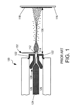
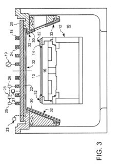
- Plasma spraying ceramic or high-temperature polymer coatings onto exposed surfaces of reactor components to promote polymer adhesion, reducing the likelihood of flaking and peeling, thus minimizing particulate contamination.
Plasma chamber and chamber component cleaning methods
PatentActiveUS11984306B2
Innovation
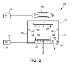
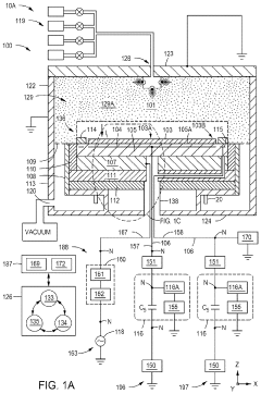
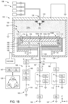
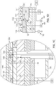
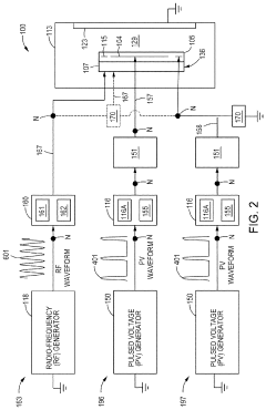
- A plasma processing system that uses pulsed voltage waveforms and an edge tuning circuit to control plasma density and uniformity, focusing ions onto the gap region for in-situ cleaning while protecting the substrate-supporting surface from damage.
Material Compatibility and Surface Quality Standards
Material compatibility is a critical factor in electropolishing processes for semiconductor and vacuum chamber applications. Stainless steel alloys, particularly 304L and 316L grades, remain the predominant materials due to their excellent corrosion resistance and favorable response to electropolishing treatments. These materials demonstrate superior performance in ultra-high vacuum (UHV) environments where outgassing must be minimized. Additionally, aluminum alloys, titanium, and copper components are increasingly utilized in specific applications where their unique properties offer advantages.
The electropolishing process must be carefully tailored to each material's specific electrochemical properties. For instance, stainless steel typically requires phosphoric-sulfuric acid electrolytes, while aluminum demands different solution compositions. This material-specific approach ensures optimal surface finish while maintaining dimensional integrity. Recent advancements have expanded compatibility to include exotic alloys such as Hastelloy and Inconel, which are gaining importance in extreme semiconductor processing environments.
Surface quality standards for electropolished components in semiconductor and vacuum applications have evolved significantly, becoming increasingly stringent. Current industry specifications typically require average roughness (Ra) values below 0.2 μm for critical components, with leading-edge applications demanding Ra values as low as 0.05 μm. Beyond roughness metrics, surface cleanliness standards now incorporate particulate contamination limits, often specified as particles per square centimeter at specific size thresholds.
Chemical cleanliness requirements have similarly intensified, with specifications limiting residual carbon, halides, and metallic contaminants to parts-per-billion levels. These standards are verified through sophisticated analytical techniques including X-ray photoelectron spectroscopy (XPS) and time-of-flight secondary ion mass spectrometry (TOF-SIMS). The semiconductor industry's transition to sub-7nm process nodes has further tightened these requirements, as even nanoscale surface defects can impact device yield.
Standardization efforts by organizations such as SEMI, ASTM, and ISO have established comprehensive test methods and acceptance criteria for electropolished surfaces. These standards address not only physical characteristics but also functional performance metrics such as vacuum compatibility and outgassing rates. The SEMI F19 specification for surface characterization of UHV components has become particularly influential, providing a framework for consistent quality assessment across the industry.
Emerging applications in quantum computing and advanced photonics are driving development of next-generation surface quality standards that incorporate additional parameters such as subsurface damage depth and crystallographic orientation effects. These evolving standards reflect the increasing sophistication of semiconductor manufacturing processes and the critical role that precisely controlled surface properties play in enabling technological advancement.
Environmental Impact and Sustainable Practices
Electropolishing processes in semiconductor and vacuum chamber applications have significant environmental implications that warrant careful consideration. Traditional electropolishing methods utilize strong acids and other hazardous chemicals that pose substantial risks to both human health and the environment. These chemicals, including phosphoric acid, sulfuric acid, and various heavy metals, can contaminate water systems and soil when improperly managed, leading to long-term ecological damage.
The industry has recognized these challenges and is actively developing more sustainable electropolishing practices. Recent innovations focus on reducing the concentration of hazardous substances in electropolishing baths while maintaining the high-quality surface finish required for semiconductor and vacuum applications. Some facilities have implemented closed-loop systems that capture, filter, and reuse electropolishing solutions, significantly reducing waste generation and fresh chemical consumption by up to 60%.
Water usage represents another critical environmental concern in electropolishing operations. Conventional processes typically require extensive rinsing stages, consuming large volumes of ultra-pure water. Advanced facilities are now implementing water recycling technologies that can reduce freshwater consumption by 40-50% through cascading rinse systems and advanced filtration technologies that enable water reuse across multiple process stages.
Energy efficiency improvements have also emerged as a focus area for sustainable electropolishing. The development of pulse electropolishing techniques has demonstrated energy savings of 25-30% compared to traditional DC electropolishing while simultaneously reducing process times. Additionally, some manufacturers have integrated renewable energy sources to power electropolishing operations, further reducing the carbon footprint of these energy-intensive processes.
Waste management practices have evolved significantly, with specialized treatment systems now capable of neutralizing and removing heavy metals and other contaminants before discharge. Progressive facilities have achieved zero liquid discharge operations through evaporation and crystallization technologies that convert liquid waste into solid residues that can be more safely handled and, in some cases, recycled to recover valuable materials.
Regulatory frameworks worldwide are increasingly stringent regarding electropolishing emissions and waste. The semiconductor industry, in particular, has established voluntary environmental performance targets that exceed regulatory requirements, driving continuous improvement in sustainable electropolishing practices. Industry collaborations have resulted in the development of standardized environmental performance metrics specifically for surface finishing operations in high-purity applications.
Unlock deeper insights with Patsnap Eureka Quick Research — get a full tech report to explore trends and direct your research. Try now!
Generate Your Research Report Instantly with AI Agent
Supercharge your innovation with Patsnap Eureka AI Agent Platform!
