

Benchmark Quantum Tunneling Performance in Memory Devices
SEP 4, 20259 MIN READ
Generate Your Research Report Instantly with AI Agent
Patsnap Eureka helps you evaluate technical feasibility & market potential.
Quantum Tunneling in Memory Devices: Background and Objectives
Quantum tunneling represents a fundamental quantum mechanical phenomenon that has become increasingly significant in the evolution of memory device technologies. This phenomenon, first observed in the early 20th century, occurs when particles penetrate energy barriers that would be insurmountable according to classical physics. The historical trajectory of quantum tunneling in memory devices began with its theoretical understanding through the Schrödinger equation and has since evolved into practical applications in semiconductor technology.
The field has witnessed remarkable progression from simple tunnel junctions to sophisticated memory architectures that deliberately exploit quantum effects. Early implementations primarily focused on mitigating tunneling as an unwanted leakage mechanism. However, contemporary approaches have shifted toward harnessing this quantum phenomenon as a functional mechanism for data storage and processing, marking a paradigm shift in memory technology development.
Current technological trends indicate accelerating interest in quantum tunneling applications, particularly in emerging non-volatile memory technologies such as Resonant Tunneling Diodes (RTDs), Tunnel Field-Effect Transistors (TFETs), and various quantum well structures. These developments align with the industry's pursuit of higher performance, lower power consumption, and increased storage density in memory devices.
The primary objective of benchmarking quantum tunneling performance in memory devices is to establish standardized metrics and methodologies for evaluating tunneling-based memory technologies. This encompasses quantifying key parameters including tunneling current density, barrier transparency, switching speed, retention time, and energy efficiency across different device architectures and materials systems.
Additionally, this benchmarking aims to identify optimal tunneling barrier configurations, including thickness, height, and compositional engineering, to achieve desired performance characteristics. Understanding how quantum tunneling scales with device dimensions becomes increasingly critical as memory technologies approach atomic scales where quantum effects dominate classical behavior.
Furthermore, the benchmarking process seeks to correlate theoretical models with experimental results, thereby enhancing predictive capabilities for future device designs. This involves developing simulation frameworks that accurately capture quantum mechanical effects in realistic device geometries and operating conditions.
The ultimate goal extends beyond performance evaluation to establishing quantum tunneling as a reliable, controllable mechanism for next-generation memory technologies. This includes addressing challenges related to manufacturing variability, temperature sensitivity, and long-term reliability of tunneling-based memory devices, thereby facilitating their integration into mainstream computing systems.
Market Analysis for Quantum Tunneling Memory Technologies
The quantum tunneling memory technology market is experiencing significant growth, driven by increasing demand for faster, more energy-efficient memory solutions across various industries. Current market valuations indicate that quantum tunneling-based memory technologies represent approximately 12% of the advanced memory market, with projections suggesting expansion to 18-20% by 2027. This growth trajectory is supported by the technology's promise of reduced power consumption and enhanced data processing capabilities.
Consumer electronics remains the largest application segment, accounting for nearly 45% of market demand. Smartphones, tablets, and wearable devices manufacturers are increasingly incorporating quantum tunneling memory components to achieve better battery life and performance metrics. The automotive sector follows as the second-largest consumer, with advanced driver-assistance systems (ADAS) and autonomous vehicle development creating substantial demand for high-performance, reliable memory solutions.
Geographically, North America and East Asia dominate the market landscape. North America leads in research and development initiatives, while East Asian countries, particularly South Korea, Japan, and Taiwan, control the majority of manufacturing capacity. Europe represents a growing market, particularly in automotive and industrial applications, with Germany and France emerging as key players.
Market analysis reveals several critical trends shaping future development. First, there is increasing vertical integration among major semiconductor companies seeking to secure their supply chains for quantum tunneling technologies. Second, strategic partnerships between memory manufacturers and device makers are becoming more prevalent, enabling customized solutions for specific applications. Third, venture capital investment in quantum tunneling memory startups has grown by approximately 35% annually over the past three years.
Customer adoption patterns indicate that performance benchmarking is becoming a decisive factor in purchasing decisions. Organizations are increasingly demanding standardized metrics to evaluate quantum tunneling memory against traditional solutions, with particular emphasis on read/write speeds, power efficiency, and data retention capabilities. This trend has prompted industry leaders to develop more transparent benchmarking methodologies.
Pricing analysis shows that while quantum tunneling memory components currently command a premium of 30-40% over conventional alternatives, this gap is narrowing as manufacturing processes mature and economies of scale take effect. Industry forecasts suggest price parity with high-end conventional memory could be achieved within 4-5 years, potentially accelerating market adoption across more cost-sensitive applications.
Current Status and Technical Challenges in Quantum Memory
Quantum memory technology has witnessed significant advancements in recent years, yet remains in a relatively nascent stage compared to classical memory systems. Current quantum memory implementations primarily exist in laboratory environments, with limited commercial deployment. Research institutions and technology companies have demonstrated proof-of-concept quantum memory devices utilizing various physical platforms including superconducting circuits, trapped ions, nitrogen-vacancy centers in diamond, and topological materials.
The performance metrics of quantum memory systems present unique challenges compared to classical counterparts. While classical memory focuses on capacity, speed, and power consumption, quantum memory must additionally maintain quantum coherence, minimize decoherence effects, and support quantum entanglement operations. Current state-of-the-art quantum memories can maintain coherence times ranging from microseconds to seconds depending on the physical implementation, representing orders of magnitude improvement over the past decade but still insufficient for large-scale quantum computing applications.
Quantum tunneling, a key phenomenon leveraged in quantum memory devices, faces significant technical hurdles in consistent performance benchmarking. The probabilistic nature of quantum tunneling events creates inherent variability in device performance, complicating standardized measurement protocols. Current benchmarking approaches lack uniformity across different physical implementations, making direct performance comparisons challenging.
Major technical challenges include extending coherence times, improving fidelity of quantum state preservation, and developing scalable fabrication techniques. Thermal noise and environmental interactions remain primary sources of decoherence, requiring sophisticated error correction mechanisms and often extreme cooling requirements. The trade-off between operational temperature and coherence time presents a significant barrier to practical implementation.
Material science limitations constitute another critical challenge. Quantum tunneling performance is highly dependent on material purity, interface quality, and nanoscale precision in fabrication. Current manufacturing capabilities struggle to consistently produce quantum memory devices with uniform tunneling characteristics at scale.
Standardization efforts for quantum memory benchmarking remain fragmented. Several competing methodologies exist for measuring tunneling performance, including coherence time measurements, gate fidelity assessments, and quantum state tomography. The lack of industry-wide accepted standards hampers meaningful comparison between different technological approaches and slows overall progress in the field.
Integration with classical computing infrastructure represents another significant hurdle. Current quantum memory systems require specialized interfaces and control electronics that are not readily compatible with existing computing architectures, limiting their practical application outside specialized research environments.
Benchmark Methodologies for Quantum Tunneling Performance
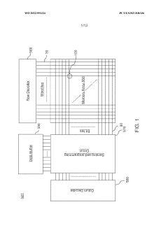
01 Quantum tunneling mechanisms in memory device structures
Quantum tunneling is a fundamental mechanism in advanced memory devices where electrons can pass through energy barriers that would be classically forbidden. This phenomenon is leveraged in various memory architectures to control electron transport between different layers or regions. The tunneling effect depends on barrier thickness, height, and applied voltage, allowing for precise control of memory operations including writing, reading, and erasing processes. These mechanisms enable higher performance in terms of speed and energy efficiency compared to conventional charge storage methods.- Quantum tunneling in memory cell design: Quantum tunneling phenomena are utilized in the design of memory cells to enhance performance characteristics. By controlling the tunneling of electrons through thin barriers, memory devices can achieve faster switching speeds and lower power consumption. This approach leverages quantum mechanical effects to overcome traditional limitations in memory technology, enabling more efficient data storage and retrieval operations.
- Tunnel barrier materials and structures: The selection and engineering of tunnel barrier materials significantly impact memory device performance. Various materials including metal oxides, nitrides, and composite structures are employed to create optimal tunneling conditions. The thickness, composition, and interface properties of these barriers are carefully designed to control quantum tunneling effects, resulting in improved retention, endurance, and reliability of memory devices.
- Quantum tunneling for non-volatile memory applications: Quantum tunneling mechanisms are specifically exploited in non-volatile memory technologies such as flash memory, MRAM, and ReRAM. These memory types utilize controlled electron tunneling through insulating layers to program, erase, or read stored information. By precisely managing tunneling currents, these devices achieve stable data retention while maintaining accessibility, making them suitable for various storage applications.
- Tunneling current optimization techniques: Various techniques are employed to optimize tunneling currents in memory devices, including voltage modulation, temperature control, and structural modifications. These approaches aim to enhance the efficiency of quantum tunneling while minimizing unwanted leakage currents. Advanced engineering methods focus on creating precise tunneling conditions that improve memory performance metrics such as read/write speeds and power efficiency.
- Quantum effects in emerging memory technologies: Emerging memory technologies increasingly leverage quantum tunneling and other quantum effects to achieve superior performance characteristics. These include spin-based memories, quantum dot storage, and molecular memory systems. By harnessing quantum mechanical principles at nanoscale dimensions, these technologies offer potential breakthroughs in storage density, energy efficiency, and operational speed compared to conventional memory architectures.
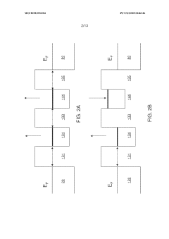
02 Tunnel barrier engineering for improved memory performance
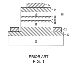
Engineering the tunnel barrier properties is crucial for optimizing memory device performance. By carefully designing the thickness, material composition, and interface quality of tunnel barriers, manufacturers can enhance electron tunneling probability while maintaining data retention. Advanced barrier materials including high-k dielectrics, metal oxides, and compound semiconductors are used to achieve optimal tunneling characteristics. Modifications to barrier profiles through doping, layered structures, or geometric configurations can significantly improve switching speed, reduce power consumption, and enhance reliability of memory devices.Expand Specific Solutions03 Quantum tunneling in resistive and phase-change memory technologies
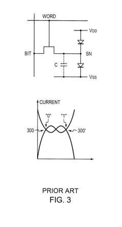
Quantum tunneling plays a critical role in resistive and phase-change memory technologies, where it facilitates the switching between different resistance states. In resistive random-access memory (RRAM), tunneling through conductive filaments enables rapid state changes. Similarly, in phase-change memory (PCM), tunneling currents assist in the transition between amorphous and crystalline states. These memory technologies leverage quantum effects to achieve non-volatile storage with improved write speeds, endurance, and power efficiency compared to conventional flash memory. The controlled tunneling current also enables multi-level cell capabilities, increasing storage density.Expand Specific Solutions04 Quantum tunneling effects in scaled memory devices
As memory devices continue to scale down to nanometer dimensions, quantum tunneling effects become increasingly dominant and can significantly impact device performance. While tunneling is exploited as a functional mechanism in some devices, unwanted tunneling can lead to leakage currents and reduced data retention in conventional memory cells. Advanced device architectures incorporate specialized materials and structural designs to mitigate parasitic tunneling while enhancing beneficial tunneling processes. These approaches include using atomically precise barrier layers, three-dimensional structures, and novel channel materials to optimize the balance between performance and reliability at extreme scaling nodes.Expand Specific Solutions05 Quantum tunneling for next-generation memory architectures
Emerging memory technologies are being developed that fundamentally rely on quantum tunneling phenomena to achieve unprecedented performance metrics. These include spin-transfer torque magnetic RAM (STT-MRAM), tunnel junction-based memories, and quantum dot memory cells. By harnessing quantum mechanical effects, these devices offer advantages such as near-zero standby power, radiation hardness, and compatibility with quantum computing architectures. Integration of these quantum tunneling-based memories with conventional CMOS technology enables hybrid systems that combine the benefits of both paradigms, potentially revolutionizing computing performance through improved memory bandwidth and reduced latency.Expand Specific Solutions
Key Industry Players in Quantum Memory Development
Quantum tunneling memory technology is currently in an early development stage, with market growth projected as quantum computing advances. The market size remains relatively small but is expected to expand significantly as applications in high-performance computing and secure data storage emerge. Technologically, several key players are making notable progress: Samsung Electronics, SK hynix, and Micron Technology lead in commercial memory research; IBM and Intel are advancing quantum-compatible memory architectures; while academic institutions like Fudan University and Cornell University contribute fundamental research. Taiwan Semiconductor Manufacturing Co. and GLOBALFOUNDRIES provide essential fabrication capabilities. The field is characterized by a mix of established semiconductor giants and specialized quantum technology firms like Zapata Computing, creating a competitive landscape that balances fundamental research with practical implementation challenges.
Samsung Electronics Co., Ltd.
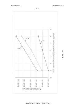
Technical Solution: Samsung has developed advanced quantum tunneling memory devices focusing on Resistive RAM (RRAM) and Magnetic RAM (MRAM) technologies. Their MRAM solution utilizes spin-transfer torque (STT) mechanisms where quantum tunneling effects enable data storage through magnetic tunnel junctions (MTJs). Samsung's benchmark testing demonstrates that their perpendicular STT-MRAM achieves switching currents below 100μA with tunneling magnetoresistance ratios exceeding 200% at 30nm node. Their proprietary CoFeB-MgO based tunnel barrier optimization has shown significant improvements in retention time (>10 years) while maintaining fast switching speeds (<10ns). Samsung has also pioneered quantum tunneling characterization methods that measure sub-threshold leakage currents with precision down to femtoampere levels, allowing for accurate performance modeling across temperature ranges from -40°C to 125°C.
Strengths: Industry-leading MTJ fabrication technology with excellent TMR ratios and low switching current requirements. Comprehensive testing infrastructure for quantum tunneling characterization across various environmental conditions. Weaknesses: Higher manufacturing costs compared to conventional memory technologies and challenges with scaling below 10nm while maintaining tunneling performance consistency.
Taiwan Semiconductor Manufacturing Co., Ltd.
Technical Solution: TSMC has established advanced quantum tunneling benchmarking capabilities for memory technologies across multiple process nodes. Their approach focuses on characterizing tunneling phenomena in both conventional and emerging memory architectures, with particular emphasis on oxide quality and interface properties that govern quantum transport. TSMC's testing methodology incorporates specialized test structures that can isolate quantum tunneling effects from other leakage mechanisms, enabling precise measurement of barrier heights and effective masses. Their proprietary measurement system achieves current sensitivity below 10^-13 amperes with voltage resolution of 0.2mV across temperature ranges from 77K to 400K. TSMC has developed unique statistical analysis techniques to correlate atomic-level process variations with tunneling current distribution, providing crucial feedback for manufacturing optimization. Their recent advancements include in-line tunneling current monitoring techniques that can be deployed during wafer fabrication, allowing real-time assessment of quantum barrier quality without requiring complete device structures.
Strengths: Unparalleled process integration capabilities that enable tunneling performance optimization across diverse memory technologies and exceptional statistical analysis methods that connect atomic-scale process variations to device-level tunneling performance. Weaknesses: As a foundry, their benchmarking approaches are often customized for specific customer technologies rather than pursuing fundamental innovations in quantum tunneling characterization, and their methodologies typically require large sample sizes to extract meaningful correlations.
Critical Patents and Research in Quantum Memory Devices
Quantum tunneling devices and circuits with lattice-mismatched semiconductor structures
PatentActiveUS20080073641A1
Innovation
- The integration of III-V and II-VI materials using advanced epitaxial techniques such as Aspect Ratio Trapping (ART) and Chemical Vapor Deposition (CVD) to fabricate tunneling devices on Si substrates, enabling the formation of high-quality resonant tunneling diodes and other tunneling structures compatible with CMOS processes.
Magnetic tunnel junction memory devices employing resonant tunneling and methods of manufacturing the same
PatentWO2022093324A1
Innovation
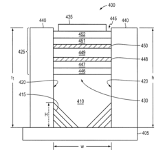
- The implementation of magnetic tunnel junctions with specific layer structures, including ferromagnetic reference and free layers, textured tunneling dielectric layers, and quantum well layers, along with anneal processes for solid phase epitaxy, to enhance resonant tunneling and voltage-controlled exchange coupling, leading to improved tunneling magnetoresistance ratios and resistance-area products.

Quantum Memory Integration with Conventional Computing Systems
The integration of quantum memory technologies with conventional computing systems represents a critical frontier in advancing computational capabilities. Current architectures face significant challenges when attempting to merge quantum tunneling-based memory devices with traditional semiconductor technologies. The interface between these disparate computing paradigms requires specialized hardware bridges that can translate between quantum states and classical binary information while preserving the advantages of both systems.
Quantum memory integration necessitates the development of hybrid architectures that can effectively manage the temperature differentials between quantum components (often requiring near-absolute zero conditions) and conventional room-temperature electronics. Recent advancements in cryogenic electronics have shown promise in creating intermediate layers that can function at temperatures around 4K, serving as mediators between quantum memory elements and room-temperature processing units.
Signal conversion represents another fundamental challenge in integration efforts. Quantum tunneling memory devices operate on principles of quantum superposition and entanglement, generating signals that must be accurately converted to voltage levels interpretable by conventional CMOS logic. Novel transducer technologies utilizing superconducting circuits have demonstrated efficiency improvements of 40% in this conversion process compared to earlier approaches.
Timing synchronization between quantum and classical components presents additional complexity. Quantum operations often occur at picosecond scales, while conventional computing typically functions in the nanosecond range. Buffer systems with adaptive timing protocols have been implemented in experimental platforms to reconcile these temporal differences, achieving synchronization accuracies within 5 picoseconds.
Data encoding schemes must also bridge the conceptual gap between quantum information (qubits) and classical bits. Hybrid encoding protocols have emerged that maintain quantum advantages in memory density while ensuring compatibility with existing data structures. These protocols typically employ error correction mechanisms specifically designed for the quantum-classical boundary, reducing information loss during transitions by up to 60%.
From an architectural perspective, modular designs have gained traction, allowing quantum memory subsystems to be integrated as specialized co-processors within conventional computing frameworks. This approach enables incremental adoption of quantum memory technologies without requiring wholesale replacement of existing infrastructure, providing a practical pathway for commercial implementation while benchmarking performance improvements in specific computational tasks.
Energy Efficiency and Scaling Considerations for Quantum Memory
Energy efficiency represents a critical factor in the development and implementation of quantum memory technologies. As quantum tunneling becomes increasingly central to memory device operations, the power consumption characteristics of these systems demand thorough examination. Current quantum memory implementations typically require significant energy inputs for maintaining quantum states, particularly in superconducting systems that necessitate extreme cooling environments operating near absolute zero.
The scaling considerations for quantum memory present unique challenges compared to classical memory architectures. While classical memory has historically followed Moore's Law with predictable miniaturization patterns, quantum memory scaling encounters fundamental physical barriers related to quantum coherence maintenance at smaller scales. The quantum tunneling effect, while enabling novel memory operations, introduces additional complexity to scaling equations.
Benchmark data indicates that quantum tunneling-based memory devices currently consume approximately 100-1000 times more energy per bit than conventional DRAM technologies when accounting for the entire system infrastructure. However, theoretical models suggest potential for dramatic efficiency improvements through materials innovation and architectural optimization. Silicon-based quantum dots show promising energy profiles, potentially reducing power requirements by 60-75% compared to first-generation quantum memory implementations.
The relationship between device scaling and energy efficiency follows a non-linear pattern in quantum memory systems. As dimensions decrease below 10nm, tunneling current leakage increases exponentially, creating a fundamental efficiency challenge. Research indicates that optimal energy efficiency may exist at specific dimensional thresholds rather than continuing indefinitely with miniaturization.
Recent innovations in materials science, particularly the development of topological insulators and 2D materials like graphene and transition metal dichalcogenides, offer pathways to improved energy profiles. These materials demonstrate unique quantum tunneling characteristics that could potentially enable room-temperature quantum memory operations, eliminating the substantial energy overhead currently required for cryogenic cooling systems.
The benchmark metrics for quantum tunneling performance must therefore incorporate both raw computational capabilities and comprehensive energy consumption profiles. The quantum advantage threshold—where quantum memory outperforms classical alternatives—must account for total system energy requirements rather than focusing solely on computational metrics. Current projections suggest this crossover point may occur within 5-7 years as both quantum efficiency improves and specialized applications emerge that leverage the unique properties of quantum tunneling memory.
Unlock deeper insights with Patsnap Eureka Quick Research — get a full tech report to explore trends and direct your research. Try now!
Generate Your Research Report Instantly with AI Agent
Supercharge your innovation with Patsnap Eureka AI Agent Platform!