How to Enhance Quantum Tunneling Behaviors in Graphene
SEP 4, 20259 MIN READ
Generate Your Research Report Instantly with AI Agent
Patsnap Eureka helps you evaluate technical feasibility & market potential.
Quantum Tunneling in Graphene: Background and Objectives
Quantum tunneling represents a fundamental quantum mechanical phenomenon where particles penetrate through energy barriers that would be insurmountable according to classical physics. In graphene, a two-dimensional carbon allotrope with hexagonal lattice structure, quantum tunneling behaviors exhibit unique characteristics due to the material's exceptional electronic properties. The historical development of quantum tunneling research in graphene can be traced back to the material's isolation in 2004, which sparked unprecedented interest in its quantum mechanical properties.
The evolution of quantum tunneling studies in graphene has progressed through several distinct phases. Initially, researchers focused on basic characterization of tunneling behaviors in pristine graphene sheets. This was followed by investigations into tunneling effects at graphene-substrate interfaces and heterojunctions. More recently, attention has shifted toward engineered tunneling phenomena through controlled defect introduction and manipulation of graphene's electronic structure.
Current technological trends indicate growing interest in harnessing enhanced quantum tunneling in graphene for practical applications. These include ultra-sensitive sensors, high-speed electronic devices, and quantum computing components. The unique band structure of graphene, featuring Dirac points where conduction and valence bands meet, creates ideal conditions for observing and manipulating quantum tunneling effects that are difficult to achieve in conventional materials.
The primary objective of enhancing quantum tunneling behaviors in graphene is to achieve precise control over tunneling parameters, including tunneling probability, directionality, and energy dependence. This control would enable the development of novel electronic devices with superior performance characteristics, particularly in terms of switching speed, energy efficiency, and information processing capabilities.
Secondary objectives include understanding the fundamental physics governing quantum tunneling in two-dimensional materials, developing standardized methods for measuring and characterizing tunneling behaviors, and establishing design principles for graphene-based quantum devices. These objectives align with broader scientific goals of expanding quantum mechanical control at the nanoscale.
The anticipated technological impact of enhanced quantum tunneling in graphene spans multiple industries, from next-generation computing architectures to advanced sensing platforms and energy conversion systems. As quantum technologies continue to mature, graphene's unique tunneling properties position it as a potential cornerstone material for quantum-enhanced devices and systems.
Market Applications and Demand Analysis for Graphene Quantum Technologies
The quantum technology market is experiencing unprecedented growth, with graphene-based quantum applications emerging as a particularly promising segment. Current market analysis indicates that the global quantum computing market is projected to reach $65 billion by 2030, with graphene-based quantum technologies potentially capturing a significant portion of this expanding market. The unique quantum tunneling properties of graphene are driving interest across multiple industries seeking competitive advantages through quantum-enhanced capabilities.
In the semiconductor industry, demand for graphene quantum tunneling applications is accelerating as traditional silicon-based technologies approach their physical limits. Major semiconductor manufacturers are actively exploring graphene's quantum properties to develop next-generation electronic components with superior performance characteristics. This transition represents a substantial market opportunity estimated at $12 billion annually by 2028.
The telecommunications sector shows strong interest in graphene-based quantum tunneling for developing ultra-secure communication systems. Quantum key distribution systems utilizing enhanced tunneling behaviors in graphene could revolutionize data security, addressing a critical market need valued at approximately $8 billion. Major telecommunications providers have already initiated research partnerships focused on commercializing these technologies within the next five years.
Medical diagnostics and imaging represent another significant market application, with quantum sensors based on graphene tunneling effects enabling unprecedented sensitivity in detecting biological markers. This application alone represents a $5 billion market opportunity, with annual growth rates exceeding 25% as healthcare systems worldwide seek more accurate and efficient diagnostic tools.
Energy storage systems benefit substantially from enhanced quantum tunneling in graphene, particularly for improving battery efficiency and capacity. The market for advanced energy storage solutions is projected to reach $546 billion by 2035, with quantum-enhanced graphene materials positioned to capture a premium segment of this market due to superior performance characteristics.
Quantum computing hardware manufacturers represent perhaps the most immediate market for enhanced graphene tunneling technologies. The ability to create more stable qubits through controlled quantum tunneling behaviors addresses a fundamental challenge in quantum computing development. Industry leaders including IBM, Google, and Microsoft have established dedicated research divisions exploring graphene-based quantum computing architectures.
Market adoption timelines vary by application, with sensing and security applications likely to reach commercialization within 3-5 years, while full-scale quantum computing applications may require 7-10 years of additional development. This staged market entry provides multiple commercialization pathways for organizations developing enhanced quantum tunneling behaviors in graphene.
Current Challenges in Graphene Quantum Tunneling Enhancement
Despite significant advancements in graphene-based quantum technologies, several critical challenges continue to impede the effective enhancement of quantum tunneling behaviors in graphene. The primary obstacle remains the precise control of tunneling barriers at the atomic scale. Current fabrication techniques struggle to create consistent nanoscale structures with the exact dimensions required for optimal tunneling effects, resulting in performance variations across devices that hinder commercial scalability.
Temperature sensitivity presents another significant challenge, as quantum tunneling phenomena in graphene are highly susceptible to thermal fluctuations. Most advanced tunneling applications require cryogenic temperatures to function effectively, limiting practical deployment in ambient environments and increasing operational costs substantially.
The interface quality between graphene and other materials critically affects tunneling behavior but remains difficult to perfect. Contamination, lattice mismatches, and defects at these interfaces create unpredictable tunneling characteristics. Even minor impurities or structural irregularities can dramatically alter the electronic properties and consequently the tunneling performance.
Measurement and characterization of quantum tunneling in graphene systems present technical difficulties that slow research progress. Current instrumentation lacks the combined spatial and temporal resolution needed to observe tunneling dynamics in real-time, particularly for complex multilayer graphene structures or hybrid systems.
Energy dissipation mechanisms in graphene tunneling junctions remain incompletely understood, leading to efficiency losses that compromise device performance. Researchers struggle to mitigate phonon scattering and other energy loss pathways that reduce tunneling probabilities and coherence times.
The theoretical modeling of quantum tunneling in graphene systems presents computational challenges due to the complex interplay between quantum confinement, electron-electron interactions, and substrate effects. Existing models often fail to accurately predict experimental results, particularly for novel device architectures or under non-equilibrium conditions.
Doping control presents another significant hurdle, as precise manipulation of carrier concentration is essential for tunneling enhancement but difficult to achieve uniformly across graphene sheets. Current doping methods often introduce additional defects or create inhomogeneous carrier distributions that adversely affect tunneling behavior.
Finally, integration challenges persist when incorporating graphene tunneling devices into conventional electronic platforms. The unique properties of graphene that enable quantum tunneling often become compromised during standard semiconductor processing steps, necessitating the development of specialized fabrication protocols that remain incompatible with mass production techniques.
State-of-the-Art Methods for Enhancing Quantum Tunneling in Graphene
01 Graphene-based quantum tunneling devices
Graphene's unique electronic properties make it ideal for quantum tunneling applications. These devices utilize the two-dimensional nature of graphene to facilitate electron tunneling between layers or across barriers. The atomically thin structure of graphene allows for precise control of tunneling behaviors, enabling the development of high-performance electronic components such as transistors, sensors, and memory devices that operate based on quantum tunneling principles.- Graphene-based quantum tunneling devices: Graphene's unique electronic properties make it an ideal material for quantum tunneling devices. These devices utilize the quantum mechanical phenomenon where electrons tunnel through potential barriers that would be insurmountable in classical physics. The atomically thin nature of graphene allows for precise control of tunneling behaviors, enabling the development of high-performance electronic components such as transistors, sensors, and memory devices with enhanced efficiency and reduced power consumption.
- Quantum tunneling effects in graphene heterostructures: Graphene heterostructures, formed by combining graphene with other 2D materials, exhibit unique quantum tunneling behaviors. These structures create potential barriers at the interfaces where electrons can tunnel through, leading to novel electronic and optical properties. By engineering the layer composition and arrangement, researchers can manipulate tunneling characteristics to create devices with tailored functionalities, including resonant tunneling diodes, photodetectors, and quantum computing components.
- Temperature and electric field effects on graphene tunneling: The quantum tunneling behavior in graphene is significantly influenced by temperature variations and applied electric fields. At lower temperatures, quantum effects become more pronounced, enhancing tunneling probabilities. Electric fields can modulate the band structure of graphene, altering the tunneling barrier height and width. These dependencies enable the development of sensitive thermal sensors, field-effect transistors, and switching devices that operate based on controlled tunneling mechanisms.
- Graphene quantum dots for tunneling applications: Graphene quantum dots (GQDs) exhibit distinctive quantum tunneling behaviors due to their confined dimensions and edge effects. These nanostructures demonstrate quantum confinement of electrons, leading to discrete energy levels and enhanced tunneling probabilities. GQDs can be incorporated into various devices to exploit their tunneling characteristics for applications in quantum computing, single-electron transistors, biosensing, and energy harvesting technologies.
- Strain-engineered tunneling in graphene systems: Mechanical strain applied to graphene significantly alters its quantum tunneling properties by modifying the electronic band structure and creating pseudomagnetic fields. This phenomenon allows for the development of strain-sensitive electronic devices where tunneling behaviors can be precisely controlled through mechanical deformation. Applications include flexible electronics, pressure sensors, and strain-tunable quantum devices that leverage the relationship between mechanical strain and electron tunneling probability.
02 Tunneling effects in graphene heterostructures
Graphene heterostructures, formed by combining graphene with other 2D materials or substrates, exhibit distinctive quantum tunneling behaviors. These structures create unique potential barriers that influence electron transport through quantum tunneling mechanisms. By engineering the interfaces between graphene and other materials, researchers can manipulate tunneling probabilities and create novel electronic states, leading to applications in quantum computing, spintronics, and ultra-sensitive detectors.Expand Specific Solutions03 Temperature and electric field effects on graphene tunneling
The quantum tunneling behavior in graphene can be significantly modulated by temperature variations and applied electric fields. These external factors affect the energy states and barrier properties in graphene structures, altering tunneling probabilities and current flow. Understanding these dependencies is crucial for designing graphene-based electronic devices that can operate reliably under various environmental conditions and for applications requiring precise control of tunneling currents.Expand Specific Solutions04 Fabrication methods for graphene tunneling structures
Various fabrication techniques have been developed to create graphene-based structures that exhibit controlled quantum tunneling behaviors. These methods include chemical vapor deposition, mechanical exfoliation, and epitaxial growth, followed by precise patterning and assembly processes. The fabrication approach significantly influences the quality of graphene layers, interface properties, and ultimately the tunneling characteristics of the resulting devices, making manufacturing methodology a critical factor in device performance.Expand Specific Solutions05 Applications of graphene quantum tunneling in electronics
Graphene's quantum tunneling properties are being leveraged for next-generation electronic applications. These include ultra-fast transistors that operate on tunneling principles rather than conventional carrier transport, highly sensitive sensors that detect minute changes in tunneling currents, and memory devices that use tunneling for data storage and retrieval. The exceptional electron mobility and tunable band gap of graphene make it particularly suitable for these applications, potentially enabling electronics with higher speeds and lower power consumption.Expand Specific Solutions
Leading Research Groups and Companies in Graphene Quantum Technologies
Quantum tunneling in graphene is currently in an early development stage, with significant research momentum but limited commercial applications. The market size is growing, driven by potential applications in quantum computing, electronics, and sensors. Technologically, academic institutions like Fudan University, Cornell University, and The University of Manchester lead fundamental research, while companies including Origin Quantum, Microsoft Technology Licensing, and Intel are advancing practical implementations. Government entities and research labs such as The Charles Stark Draper Laboratory and Advanced Industrial Science & Technology provide critical infrastructure support. The field is characterized by cross-sector collaboration between academia, industry, and government, with Asian institutions particularly active in experimental breakthroughs.
Origin Quantum Computing Technology (Hefei) Co., Ltd.
Technical Solution: Origin Quantum has developed a distinctive approach to enhancing quantum tunneling behaviors in graphene through their "Graphene Quantum Coherent Transport" platform. Their technique focuses on creating precisely engineered quantum dots in graphene through a combination of electrostatic gating and nanolithography[1]. The company has pioneered methods to create atomically precise edges in graphene nanostructures, which significantly enhances quantum tunneling effects by reducing edge scattering. Their approach involves creating tunable tunnel barriers using local electrostatic gates that can modulate the potential landscape with exceptional precision, allowing for dynamic control of tunneling rates[2]. Origin Quantum has also developed specialized low-temperature measurement systems that can characterize quantum tunneling behaviors with high energy resolution while maintaining quantum coherence. Their recent advancements include creating coupled quantum dot arrays in graphene where tunneling can be coherently controlled, potentially forming the basis for quantum information processing applications[3].
Strengths: Strong focus on quantum applications gives deep expertise in quantum coherent phenomena; significant government support for quantum technologies in China; integrated approach combining materials science, nanofabrication, and quantum physics. Weaknesses: Relatively newer entrant compared to some established players; techniques currently limited to laboratory-scale demonstrations; challenges in maintaining consistent quantum tunneling behaviors across different graphene samples.
The University of Manchester
Technical Solution: The University of Manchester has pioneered significant advancements in enhancing quantum tunneling behaviors in graphene through their development of van der Waals heterostructures. Their approach involves creating precisely engineered multilayer structures where graphene is sandwiched between hexagonal boron nitride (hBN) layers, allowing for controlled manipulation of quantum tunneling effects[1]. Their researchers have demonstrated that by applying perpendicular electric fields to these heterostructures, they can modulate the tunneling current with exceptional precision. The university has also developed techniques to create atomically clean interfaces between graphene and other 2D materials, which is crucial for preserving the quantum coherence necessary for tunneling phenomena[2]. Their recent work has focused on exploiting resonant tunneling in graphene-based structures, achieving negative differential resistance and demonstrating potential for high-frequency oscillators operating in the terahertz range[3].
Strengths: World-leading expertise in graphene research (home of Nobel Prize winners Geim and Novoselov); exceptional capabilities in creating high-quality heterostructures with atomically clean interfaces; strong track record of experimental breakthroughs in quantum transport. Weaknesses: Some techniques require extremely specialized equipment and ultra-high vacuum conditions, limiting commercial scalability; challenges remain in maintaining consistent tunneling behaviors across larger graphene sheets.
Critical Patents and Research Breakthroughs in Graphene Tunneling
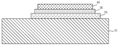
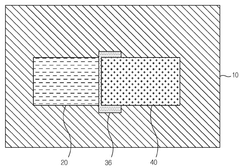
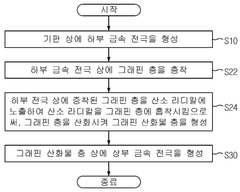
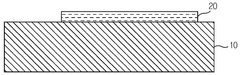
Quantum device and manufacturing method therefor
PatentWO2025105586A1
Innovation
- The use of graphene oxide with insulating properties as the insulating layer in quantum devices, which can be formed to maintain a consistent and low thickness, compatible with existing semiconductor processes, thereby optimizing the thickness and quality of the insulating layer.
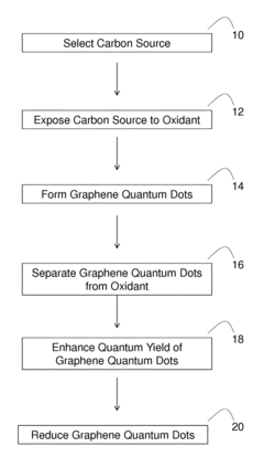
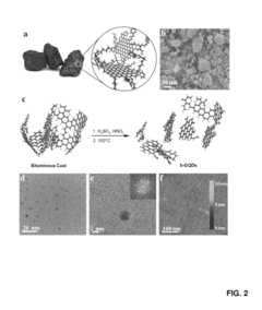
Methods of producing graphene quantum dots from coal and coke
PatentActiveUS9919927B2
Innovation
- A method involving exposing carbon sources like coal, coke, or their combinations to oxidants, such as a mixture of sulfuric and nitric acid, followed by separation, reduction, and enhancement processes to produce graphene quantum dots with controlled sizes and improved quantum yield.
Fabrication Techniques and Material Engineering Considerations
The fabrication of graphene structures with enhanced quantum tunneling properties requires precise control at the nanoscale level. Chemical vapor deposition (CVD) remains the predominant method for producing high-quality graphene sheets suitable for quantum applications. Recent advancements in CVD techniques have enabled the growth of graphene with controlled defect densities, which significantly influence tunneling behaviors. Temperature gradients during the growth process can be manipulated to create regions with varying electron mobility, directly affecting tunneling probabilities across potential barriers.
Molecular beam epitaxy (MBE) offers an alternative approach with exceptional precision for creating atomically thin graphene heterostructures. The layer-by-layer deposition allows for the engineering of quantum wells and barriers with atomic precision, creating ideal conditions for observing and enhancing quantum tunneling phenomena. The interface quality between graphene and substrate materials critically determines the coherence length of electron waves, with higher coherence facilitating more efficient tunneling processes.
Strain engineering has emerged as a powerful technique for modulating graphene's electronic properties. By applying controlled mechanical deformation to graphene sheets, researchers can create pseudomagnetic fields exceeding 300 Tesla, dramatically altering the tunneling landscape. Nanopatterning techniques, including electron beam lithography and helium ion microscopy, enable the creation of quantum constrictions and barriers with dimensions below 10 nm, where quantum effects become pronounced.
Doping strategies represent another crucial aspect of engineering quantum tunneling behaviors. Substitutional doping with nitrogen or boron atoms modifies the local electronic structure, creating potential wells or barriers that electrons can tunnel through. Electrostatic doping through proximity effects with carefully selected substrate materials offers a non-invasive alternative that preserves graphene's intrinsic mobility while still enabling tunneling modulation.
The integration of graphene with other 2D materials in van der Waals heterostructures presents perhaps the most promising frontier for tunneling enhancement. By creating atomically thin stacks of graphene with materials like hexagonal boron nitride (h-BN) or transition metal dichalcogenides (TMDCs), researchers can engineer precise quantum tunneling junctions with tailored barrier heights and widths. The crystallographic alignment between layers critically influences the resulting tunneling characteristics, with specific twist angles creating moiré patterns that dramatically modify the electronic landscape.
Post-fabrication treatments, including thermal annealing and plasma processing, can further optimize tunneling behaviors by removing contaminants and healing structural defects that might otherwise scatter tunneling electrons. Cryogenic processing environments have proven essential for preserving the quantum coherence necessary for reliable tunneling experiments and applications.
Environmental and Scalability Factors in Graphene Quantum Devices
The environmental conditions surrounding graphene quantum devices significantly impact their quantum tunneling behaviors and overall performance. Temperature fluctuations represent a primary concern, as quantum tunneling effects in graphene are highly temperature-dependent. At higher temperatures, thermal noise can disrupt the coherence of quantum states, reducing tunneling efficiency. Conversely, extremely low temperatures (near absolute zero) enhance quantum coherence but introduce substantial operational challenges for practical applications outside laboratory settings.
Electromagnetic interference presents another critical environmental factor affecting graphene quantum devices. External electromagnetic fields can perturb the delicate quantum states necessary for tunneling phenomena, necessitating sophisticated shielding solutions. This becomes particularly challenging when considering the integration of graphene quantum devices with conventional electronics in real-world applications.
Substrate interactions also play a decisive role in quantum tunneling behaviors. The choice of substrate material can introduce strain, impurities, or charge puddles that modify graphene's electronic properties. Recent research indicates that hexagonal boron nitride (h-BN) substrates minimize these detrimental effects, preserving graphene's intrinsic quantum properties more effectively than traditional silicon dioxide substrates.
Regarding scalability, several significant challenges emerge when transitioning from laboratory demonstrations to industrial-scale production. Maintaining structural uniformity across larger graphene sheets remains problematic, as defects and grain boundaries can disrupt quantum tunneling pathways. Current fabrication techniques struggle to produce consistent quantum behavior across wafer-scale graphene implementations.
Integration density represents another scalability concern. As device dimensions shrink to enhance quantum effects, interconnect challenges and cross-talk between adjacent quantum components become increasingly problematic. This necessitates novel architectural approaches that balance quantum performance with practical integration requirements.
The economic viability of scaled production presents perhaps the most significant barrier to widespread adoption. Current methods for producing high-quality graphene suitable for quantum applications remain costly and time-intensive. Advances in chemical vapor deposition and epitaxial growth techniques show promise for reducing production costs, but significant improvements in throughput and quality consistency are still required before graphene quantum devices can achieve commercial viability at scale.
Unlock deeper insights with Patsnap Eureka Quick Research — get a full tech report to explore trends and direct your research. Try now!
Generate Your Research Report Instantly with AI Agent
Supercharge your innovation with Patsnap Eureka AI Agent Platform!