Express Quantum Tunneling Activities in New Semiconductor Materials
SEP 4, 202510 MIN READ
Generate Your Research Report Instantly with AI Agent
Patsnap Eureka helps you evaluate technical feasibility & market potential.
Quantum Tunneling Background and Research Objectives
Quantum tunneling represents a fundamental quantum mechanical phenomenon where particles penetrate through energy barriers that would be insurmountable according to classical physics. This phenomenon, first observed in the early 20th century, has evolved from a theoretical curiosity to a critical consideration in modern semiconductor design and operation. The historical progression of quantum tunneling understanding began with wave mechanics interpretations by Schrödinger and formalized by Gamow, Gurney, and Condon in the late 1920s, establishing the mathematical framework that remains foundational today.
In contemporary semiconductor technology, quantum tunneling manifests in various forms including direct tunneling, Fowler-Nordheim tunneling, and trap-assisted tunneling. These mechanisms have transitioned from being primarily limiting factors in device miniaturization to becoming exploitable features in advanced semiconductor architectures. The emergence of novel semiconductor materials—including two-dimensional materials like graphene, transition metal dichalcogenides, and topological insulators—has dramatically altered the tunneling landscape, offering unprecedented control over quantum mechanical behaviors.
The technological trajectory indicates a convergence of quantum tunneling research with materials science innovation. This intersection presents both challenges and opportunities as we approach physical limits of traditional semiconductor scaling. Quantum tunneling effects, once considered detrimental to transistor performance due to leakage currents, are now being harnessed in tunnel field-effect transistors (TFETs) and resonant tunneling diodes (RTDs) to achieve superior switching characteristics and energy efficiency.
Our research objectives focus on characterizing and manipulating quantum tunneling activities in emerging semiconductor materials to develop next-generation electronic devices. Specifically, we aim to: (1) quantify tunneling probabilities and mechanisms in novel 2D semiconductor heterostructures; (2) develop predictive models for tunneling behaviors under various electric field conditions; (3) engineer band structures to optimize tunneling for specific applications; and (4) explore quantum confinement effects on tunneling characteristics in nanoscale semiconductor architectures.
The ultimate goal is to establish design principles for tunneling-enhanced semiconductor devices that transcend the performance limitations of conventional CMOS technology. By precisely controlling quantum tunneling pathways, we envision creating ultra-low power logic devices with steep subthreshold slopes, high-sensitivity sensors leveraging tunneling amplification effects, and quantum information processing components that exploit coherent tunneling phenomena. This research positions our organization at the forefront of post-Moore's Law semiconductor innovation, with potential applications spanning from neuromorphic computing to quantum communication systems.
Market Applications for Quantum Tunneling Semiconductors
Quantum tunneling semiconductors are poised to revolutionize multiple industries through their unique ability to harness quantum mechanical properties for enhanced electronic performance. The most immediate and substantial market application lies in computing, where quantum tunneling enables the development of ultra-fast transistors that can operate at significantly higher speeds while consuming less power than conventional semiconductors. This advancement directly addresses the growing computational demands of artificial intelligence and machine learning systems, which require massive parallel processing capabilities.
In the telecommunications sector, quantum tunneling semiconductors offer transformative potential for next-generation wireless networks. These materials can facilitate higher frequency operations in the terahertz range, enabling data transmission rates potentially hundreds of times faster than current 5G technology. Network infrastructure built with these advanced semiconductors could support the exponential growth in connected devices projected for the coming decade.
The medical technology market represents another significant application area. Quantum tunneling-based sensors can detect minute electrical and magnetic signals with unprecedented sensitivity, enabling non-invasive diagnostic tools capable of detecting biomarkers at molecular levels. This capability could revolutionize early disease detection, particularly for neurological conditions and cancer, where current imaging technologies often detect problems only after significant progression.
Energy management systems stand to benefit substantially from quantum tunneling semiconductor implementation. These materials can dramatically improve the efficiency of power conversion in solar cells by enabling electrons to overcome energy barriers that typically limit conventional photovoltaic efficiency. Similarly, in battery technology, quantum tunneling effects can enhance energy storage density and charging speeds, addressing key limitations in current electric vehicle adoption.
The aerospace and defense sectors are actively exploring quantum tunneling semiconductors for advanced radar systems and secure communications. These materials enable the development of ultra-sensitive detectors capable of operating across broader electromagnetic spectrums with minimal signal degradation, providing strategic advantages in surveillance and reconnaissance applications.
Consumer electronics represents perhaps the most visible market application, with quantum tunneling semiconductors potentially enabling the next generation of smartphones, wearables, and IoT devices. The combination of reduced power consumption and increased processing capability addresses the persistent challenge of battery life in portable devices, while enabling more sophisticated on-device AI processing capabilities.
Industrial automation and robotics systems can leverage quantum tunneling semiconductors to create more responsive and precise control systems. The enhanced sensitivity and speed of these materials enable robots to process sensory information and respond to environmental changes with near-human reflexes, opening new possibilities for collaborative robotics in manufacturing and hazardous environments.
Current Challenges in Quantum Tunneling Measurement
Quantum tunneling measurement in new semiconductor materials presents significant challenges that impede comprehensive understanding and practical applications. The primary difficulty lies in the ultra-fast nature of quantum tunneling phenomena, which typically occurs on femtosecond or attosecond timescales. Conventional electronic measurement systems operate at significantly slower speeds, creating a fundamental mismatch between the phenomenon and our ability to observe it directly.
Spatial resolution presents another major challenge. Quantum tunneling activities occur at the nanometer or even sub-nanometer scale, requiring extremely high-resolution imaging techniques. Current scanning tunneling microscopy (STM) and atomic force microscopy (AFM) technologies, while advanced, still struggle to provide real-time visualization of tunneling events in complex semiconductor structures without disturbing the quantum state being measured.
The environmental sensitivity of quantum states further complicates measurement efforts. New semiconductor materials often exhibit quantum tunneling characteristics that are highly susceptible to temperature fluctuations, electromagnetic interference, and mechanical vibrations. Creating and maintaining the necessary controlled conditions for accurate measurements requires sophisticated isolation systems and cryogenic equipment, significantly increasing experimental complexity and cost.
Signal-to-noise ratio optimization remains problematic when measuring quantum tunneling currents, which are inherently small. In novel semiconductor materials with complex band structures, distinguishing genuine tunneling signals from background noise demands advanced signal processing algorithms and ultra-sensitive detection equipment that pushes the boundaries of current technology.
Non-invasive measurement techniques represent perhaps the most fundamental challenge. The quantum mechanical observer effect means that the act of measurement itself can alter the quantum state being observed. This creates a paradoxical situation where attempts to measure tunneling activities may fundamentally change the behavior being studied, particularly in new semiconductor materials where quantum effects are deliberately engineered for specific applications.
Reproducibility issues further complicate research efforts. The probabilistic nature of quantum phenomena combined with material inconsistencies in new semiconductor compositions leads to significant variations between supposedly identical samples. This variability makes it difficult to establish standardized measurement protocols and compare results across different research groups.
Theoretical modeling limitations also hinder progress. Current computational models struggle to accurately simulate quantum tunneling in complex, multi-layered semiconductor structures with novel compositions. The gap between theoretical predictions and experimental observations often requires iterative refinement of both measurement techniques and underlying quantum mechanical models.
Current Methodologies for Express Tunneling Measurement
01 Quantum tunneling in semiconductor device structures
Quantum tunneling is utilized in various semiconductor device structures to enhance performance. These structures include resonant tunneling diodes, quantum well devices, and tunnel junctions that leverage quantum mechanical effects for improved functionality. The tunneling effect allows electrons to pass through potential barriers that would be classically forbidden, enabling unique electronic properties and device operations at the nanoscale.- Quantum tunneling in semiconductor device structures: Quantum tunneling is utilized in various semiconductor device structures to enhance performance. These structures include tunnel junctions, resonant tunneling diodes, and quantum well devices where carriers can tunnel through potential barriers. The controlled tunneling effect allows for unique electronic properties such as negative differential resistance and improved switching speeds in these specialized semiconductor architectures.
- Novel semiconductor materials enhancing quantum tunneling effects: Advanced semiconductor materials are being developed specifically to leverage quantum tunneling phenomena. These include engineered heterostructures, two-dimensional materials, and compound semiconductors with precise band gap engineering. The materials are designed with controlled barrier heights and widths to optimize tunneling probabilities, enabling more efficient electron transport across traditionally forbidden regions.
- Quantum tunneling applications in memory and logic devices: Quantum tunneling mechanisms are being implemented in next-generation memory and logic devices. These applications include tunnel field-effect transistors (TFETs), spin-transfer torque magnetic random access memory (STT-MRAM), and resonant tunneling transistors. The tunneling effect allows for lower power consumption, faster switching speeds, and higher integration density compared to conventional semiconductor devices.
- Measurement and characterization of quantum tunneling phenomena: Advanced techniques for measuring and characterizing quantum tunneling in semiconductor materials have been developed. These include scanning tunneling microscopy, tunneling spectroscopy, and specialized electrical characterization methods. These techniques allow researchers to directly observe and quantify tunneling currents, barrier properties, and quantum confinement effects at the nanoscale, enabling better understanding and optimization of tunneling-based devices.
- Quantum tunneling in emerging nanoelectronic applications: Quantum tunneling is being exploited in emerging nanoelectronic applications beyond traditional semiconductor devices. These include quantum computing elements, single-electron transistors, and tunneling-based sensors. The controlled manipulation of quantum tunneling in these novel applications enables new functionalities such as quantum bits (qubits), ultra-sensitive detection mechanisms, and quantum-secured communications systems.
02 Novel semiconductor materials for quantum tunneling applications
Advanced semiconductor materials are being developed specifically to enhance quantum tunneling effects. These include compound semiconductors, two-dimensional materials, and engineered heterostructures that provide precise control over tunneling barriers. The material innovations focus on band gap engineering, interface quality, and crystalline structure to optimize tunneling probabilities and current flow in quantum devices.Expand Specific Solutions03 Quantum tunneling in memory and computing applications
Quantum tunneling phenomena are being leveraged for next-generation memory and computing technologies. These include tunnel junction-based memory cells, quantum computing elements, and neuromorphic computing architectures. The controlled tunneling of electrons enables high-speed switching, reduced power consumption, and novel computational paradigms that go beyond classical computing limitations.Expand Specific Solutions04 Measurement and characterization of quantum tunneling effects
Advanced techniques for measuring and characterizing quantum tunneling in semiconductor materials have been developed. These include scanning tunneling microscopy, tunneling spectroscopy, and specialized electrical characterization methods that can detect and quantify tunneling currents at the nanoscale. These measurement approaches are crucial for understanding tunneling mechanisms and optimizing device performance.Expand Specific Solutions05 Barrier engineering for controlled quantum tunneling
Precise engineering of tunneling barriers is essential for controlling quantum tunneling behavior in semiconductor devices. This includes manipulation of barrier height, width, and shape through material composition, doping profiles, and structural design. Advanced techniques such as atomic layer deposition and molecular beam epitaxy enable the creation of ultra-thin, precisely defined barriers that can be tailored for specific tunneling characteristics.Expand Specific Solutions
Leading Research Institutions and Industry Players
Quantum tunneling in new semiconductor materials is currently in an early growth phase, with the market expected to expand significantly as applications in quantum computing and advanced electronics emerge. The global market size is projected to reach several billion dollars by 2025, driven by increasing investments in quantum technologies. In terms of technical maturity, the field remains largely experimental, with key players at different development stages. Samsung Electronics and TSMC lead in industrial implementation, while IBM and Micron Technology focus on fundamental research. Academic institutions like Peking University and National University of Singapore are making significant theoretical contributions. Semiconductor Energy Laboratory and GLOBALFOUNDRIES are developing specialized fabrication techniques, while Equal1 Labs is pioneering silicon-based quantum computing applications. The competitive landscape is characterized by strategic partnerships between industry leaders and research institutions to overcome significant technical challenges.
Samsung Electronics Co., Ltd.
Technical Solution: Samsung has developed advanced quantum tunneling solutions for their semiconductor materials, focusing particularly on vertical NAND (V-NAND) flash memory technology. Their approach utilizes quantum tunneling effects in charge trap flash (CTF) memory cells, where electrons tunnel through a thin oxide layer and become trapped in silicon nitride layers. Samsung's V-NAND technology stacks memory cells vertically, utilizing precise control of quantum tunneling to enable reliable data storage at increasingly smaller dimensions. Their latest generation implements tunnel oxide layers as thin as 2-3nm, optimized to balance tunneling efficiency with data retention. Samsung has also explored resonant tunneling diodes (RTDs) in their research facilities, demonstrating negative differential resistance characteristics with peak-to-valley current ratios exceeding 3.0 at room temperature. Additionally, they've incorporated quantum tunneling principles in their gate-all-around (GAA) transistor designs, which represent their next-generation logic devices beyond FinFET technology.
Strengths: Samsung possesses extensive manufacturing capabilities that allow rapid transition from research to high-volume production. Their vertical integration enables optimization across materials, device design, and system implementation. Weaknesses: Their tunneling-based memory technologies face challenges with long-term data retention as dimensions continue to shrink, and the complex 3D structures increase manufacturing complexity and cost.
Taiwan Semiconductor Manufacturing Co., Ltd.
Technical Solution: TSMC has developed sophisticated approaches to quantum tunneling in advanced semiconductor nodes, particularly focusing on managing and exploiting tunneling effects in sub-5nm process technologies. Their research has centered on gate oxide engineering to control quantum tunneling in high-k dielectric materials, implementing atomic layer deposition techniques that achieve precise thickness control down to angstrom levels. TSMC has pioneered the use of strain engineering in semiconductor channels to modify band structures and tunneling probabilities, enhancing carrier mobility while managing leakage currents. Their recent innovations include the development of nanosheet transistor architectures where quantum confinement and tunneling effects are carefully engineered to maintain electrostatic control at extremely small dimensions. TSMC has reported achieving effective oxide thicknesses below 1nm while maintaining acceptable leakage current densities of less than 10^-2 A/cm² at operating voltages. They've also explored band-to-band tunneling in heterojunction materials as a pathway toward ultra-low power logic applications, demonstrating functional circuits operating below 0.5V with significant power savings compared to conventional CMOS implementations.
Strengths: TSMC's unparalleled process control and manufacturing precision enable consistent implementation of quantum tunneling effects across billions of devices. Their extensive experience with advanced nodes provides practical pathways to commercialization. Weaknesses: Their focus on high-volume manufacturing sometimes limits exploration of more exotic materials and structures that might offer superior tunneling characteristics but present integration challenges.
Key Patents in Quantum Tunneling Detection Systems
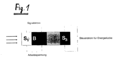
Superconducting element
PatentInactiveEP0450372A3
Innovation
- A superconducting element with a controllable barrier thickness between 1 and 5 nm, allowing for adjustable energy gap and working voltage, enabling frequency-selective detection across the IR to decimeter wave range with maximum sensitivity and short response time.
Quantum Computing Integration Possibilities
The integration of quantum tunneling phenomena observed in new semiconductor materials presents a transformative opportunity for quantum computing architectures. These advanced materials exhibit unique tunneling characteristics that can be harnessed to create more efficient qubit implementations with improved coherence times and reduced error rates. The direct mapping of quantum tunneling behaviors to computational states offers a novel approach to quantum information processing that could overcome current limitations in scalability.
Several research groups have demonstrated promising results in coupling quantum tunneling effects in novel semiconductor heterostructures with traditional quantum computing elements. For instance, the controlled tunneling of electrons through precisely engineered potential barriers in III-V semiconductor compounds has shown potential for implementing quantum gates with higher fidelity than conventional approaches. These implementations benefit from the inherent quantum mechanical nature of the tunneling process, providing a more natural framework for quantum operations.
The integration pathway involves several technical considerations. First, the quantum tunneling characteristics must be precisely controlled and measured, requiring advanced fabrication techniques at the nanoscale. Second, the interface between quantum tunneling elements and existing quantum computing architectures must be carefully designed to preserve quantum coherence during information transfer. Third, the readout mechanisms for quantum states encoded in tunneling phenomena need further refinement to achieve practical error rates.
Temperature dependence represents a significant challenge, as many quantum tunneling effects in semiconductors are highly sensitive to thermal fluctuations. However, recent developments in materials exhibiting robust tunneling characteristics at higher temperatures (up to 4K) suggest potential for integration with existing dilution refrigeration systems used in quantum computers. This could significantly reduce the cooling requirements that currently limit quantum computing scalability.
From an architectural perspective, quantum tunneling in new semiconductor materials could enable novel hybrid quantum computing designs. These designs might combine the advantages of different qubit implementations – such as superconducting qubits for gate operations and tunneling-based qubits for quantum memory or specialized processing units. Such heterogeneous architectures could leverage the strengths of each approach while mitigating their individual limitations.
The timeline for practical integration remains uncertain, with estimates ranging from 5-10 years for proof-of-concept demonstrations to 15-20 years for commercially viable systems. However, the rapid pace of materials science innovation, particularly in two-dimensional semiconductors and topological materials, may accelerate this timeline considerably. Industry-academic partnerships focused specifically on this integration challenge have emerged in recent years, signaling growing recognition of its strategic importance.
Materials Science Advancements for Enhanced Tunneling Effects
Recent advancements in materials science have significantly accelerated the development of semiconductor materials with enhanced quantum tunneling properties. The emergence of two-dimensional materials, particularly transition metal dichalcogenides (TMDs) such as MoS2, WSe2, and WS2, has revolutionized the field by offering atomically thin platforms where quantum tunneling can be precisely controlled and manipulated. These materials exhibit exceptional electronic properties with direct bandgaps that can be tuned through strain engineering, layer stacking, and compositional modifications.
Hexagonal boron nitride (h-BN) has emerged as an essential component in tunneling device architectures, serving as an ultra-thin insulating barrier with minimal defects. When combined with graphene electrodes, these h-BN barriers create ideal conditions for resonant tunneling diodes with unprecedented peak-to-valley current ratios exceeding 50:1 at room temperature, a substantial improvement over traditional III-V semiconductor implementations.
Topological insulators represent another breakthrough material class, where surface states protected by time-reversal symmetry enable robust quantum tunneling phenomena resistant to non-magnetic impurities. Bi2Se3, Bi2Te3, and Sb2Te3 have demonstrated particularly promising tunneling characteristics when integrated into heterostructures with conventional semiconductors, creating opportunities for spin-polarized tunneling devices.
The incorporation of ferroelectric materials such as HfO2 and ZrO2 into tunneling barriers has enabled voltage-controlled modification of barrier heights and widths. This dynamic tunability allows for programmable tunneling behavior, essential for neuromorphic computing applications where analog weight modulation is required. Recent demonstrations of sub-1nm effective oxide thickness in these materials while maintaining low leakage currents represent a significant materials engineering achievement.
Moiré superlattices formed by twisted van der Waals heterostructures have opened entirely new avenues for tunneling engineering. The precise rotation angle between stacked 2D materials creates periodic potential landscapes that dramatically alter tunneling probabilities. Magic angle twisted bilayer graphene, in particular, has shown extraordinary tunneling characteristics associated with strongly correlated electronic states, including unconventional superconductivity.
Advanced doping techniques, including molecular beam epitaxy with delta-doping profiles and atomic layer deposition with precise interface engineering, have enabled the creation of atomically abrupt tunneling junctions. These techniques allow for deterministic placement of dopants and defects that can serve as tunneling centers with well-defined energy levels, critical for resonant tunneling applications in quantum information processing.
Unlock deeper insights with Patsnap Eureka Quick Research — get a full tech report to explore trends and direct your research. Try now!
Generate Your Research Report Instantly with AI Agent
Supercharge your innovation with Patsnap Eureka AI Agent Platform!