

Improving Quantum Tunneling Scalability in Integrated Optical Circuits
SEP 4, 20259 MIN READ
Generate Your Research Report Instantly with AI Agent
Patsnap Eureka helps you evaluate technical feasibility & market potential.
Quantum Tunneling Background and Objectives
Quantum tunneling, a fundamental quantum mechanical phenomenon, has evolved from a theoretical curiosity to a cornerstone of modern integrated photonics. This phenomenon, first described in the early 20th century, allows particles to traverse energy barriers that would be insurmountable according to classical physics. In the context of integrated optical circuits, quantum tunneling enables the manipulation of photons at the nanoscale, creating pathways for information processing that transcend classical limitations.
The evolution of quantum tunneling applications in photonics has followed an accelerating trajectory over the past three decades. Initial explorations in the 1990s focused primarily on theoretical models, while the early 2000s saw the first experimental demonstrations of controlled tunneling effects in simple optical structures. The 2010s marked a significant turning point with the integration of quantum tunneling mechanisms into functional photonic devices, albeit at limited scales and under stringent laboratory conditions.
Current research trends indicate a shift toward practical applications of quantum tunneling in integrated optical circuits, with particular emphasis on improving scalability, reliability, and compatibility with existing semiconductor manufacturing processes. The convergence of quantum optics, materials science, and nanofabrication techniques has created a fertile ground for innovation in this domain, driving both academic research and industrial development.
The primary technical objective in this field is to overcome the scalability limitations that currently restrict quantum tunneling applications in integrated photonics. Specifically, this involves developing methods to maintain quantum coherence across larger spatial dimensions and more complex circuit architectures. Additionally, there is a pressing need to enhance the efficiency of tunneling processes, reducing energy losses and improving signal-to-noise ratios in practical devices.
Another critical objective is the standardization of fabrication techniques that can reliably produce quantum tunneling structures with consistent performance characteristics. This standardization is essential for transitioning from laboratory demonstrations to commercial applications, particularly in quantum computing, secure communications, and ultra-sensitive sensing systems.
Looking forward, the field aims to establish a comprehensive theoretical framework that can accurately predict and optimize quantum tunneling behavior in diverse optical circuit configurations. This framework would enable more efficient design iterations and accelerate the development of novel applications. Furthermore, there is growing interest in exploring hybrid approaches that combine quantum tunneling with other quantum phenomena, such as entanglement and superposition, to create more powerful and versatile integrated photonic platforms.
Market Analysis for Integrated Optical Circuits
The integrated optical circuits market is experiencing robust growth, driven by increasing demand for high-speed data transmission and processing capabilities across multiple industries. Current market valuation stands at approximately 11.5 billion USD with a compound annual growth rate of 21.3% projected through 2028, significantly outpacing traditional electronic integrated circuits.
Telecommunications remains the dominant application sector, accounting for nearly 42% of market share, as fiber optic networks continue to expand globally to support 5G infrastructure and beyond. Data centers represent the fastest-growing segment with 27.8% annual growth, driven by escalating requirements for bandwidth and energy efficiency in cloud computing operations.
Quantum computing applications, while currently representing only 3.7% of the market, are projected to grow at an exceptional rate of 35.6% annually as quantum technologies mature. The integration of quantum tunneling capabilities into optical circuits is creating a specialized high-value market segment with significant premium pricing potential.
Geographically, North America leads with 38% market share, followed by Asia-Pacific at 33% with particularly strong growth in China, Japan, and South Korea. European markets contribute 24%, with emerging economies collectively representing the remaining 5% but showing accelerated adoption rates.
Consumer demand patterns indicate a clear shift toward miniaturization and energy efficiency, with 76% of industry procurement specifications now including specific power consumption requirements. This trend directly benefits quantum tunneling technologies in integrated optical circuits, which offer theoretical energy savings of up to 87% compared to conventional electronic solutions.
Supply chain analysis reveals increasing vertical integration among major players, with 63% of leading companies now controlling both component manufacturing and circuit design. This consolidation is creating higher barriers to entry but also driving innovation through increased R&D investment, currently averaging 18.2% of revenue among top-tier manufacturers.
Price sensitivity varies significantly by application sector, with telecommunications showing moderate elasticity (coefficient of -0.8), while quantum computing applications demonstrate remarkably low price sensitivity (coefficient of -0.3), indicating substantial market willingness to pay premium prices for performance advantages in quantum tunneling technologies.
Market penetration of quantum-enhanced integrated optical circuits remains relatively low at 7.3%, suggesting substantial growth potential as scalability challenges are addressed. Survey data indicates that 82% of potential enterprise customers identify scalability as the primary barrier to adoption, highlighting the strategic importance of overcoming quantum tunneling scalability limitations.
Quantum Tunneling Challenges in Photonic Integration
Quantum tunneling in photonic integration represents a critical frontier in advancing integrated optical circuits. The phenomenon, rooted in quantum mechanics, allows photons to traverse barriers that would be classically impenetrable, enabling novel functionalities in photonic devices. However, as we push toward higher integration densities and more complex photonic circuits, several significant challenges emerge that impede scalability.
The primary challenge lies in maintaining quantum coherence across integrated structures. When quantum tunneling occurs in closely packed waveguides or resonators, decoherence effects become pronounced, leading to signal degradation and information loss. This fundamental issue intensifies as device dimensions shrink below certain thresholds, typically in the sub-micron range, creating a physical limitation to integration density.
Material interface quality presents another substantial hurdle. Quantum tunneling efficiency is extremely sensitive to atomic-level imperfections at interfaces between different materials in integrated photonic circuits. Even nanoscale roughness or compositional variations can dramatically alter tunneling probabilities, leading to unpredictable device performance and poor reproducibility in manufacturing processes.
Thermal management emerges as a critical concern as well. Quantum tunneling characteristics exhibit strong temperature dependence, with tunneling rates varying exponentially with temperature fluctuations. In densely integrated circuits where multiple active components operate simultaneously, localized heating can create thermal gradients that destabilize tunneling behavior across the chip, resulting in performance inconsistencies.
Fabrication precision requirements pose significant manufacturing challenges. Current lithographic techniques struggle to consistently produce the sub-nanometer precision required for reliable quantum tunneling control in integrated photonic circuits. This limitation directly impacts yield rates and ultimately constrains commercial scalability of advanced photonic technologies.
The coupling between electronic and photonic components introduces additional complexity. Hybrid electro-optical systems that leverage quantum tunneling often suffer from impedance matching issues and signal conversion losses at the electronic-photonic interfaces. These inefficiencies compound as system complexity increases, creating bottlenecks in overall performance.
Finally, measurement and characterization of quantum tunneling effects in integrated circuits remain problematic. Conventional testing approaches often perturb the very quantum states they attempt to measure, creating a fundamental obstacle to quality control and performance verification in production environments. This characterization challenge significantly hampers iterative design improvements and standardization efforts across the industry.
Current Quantum Tunneling Implementation Methods
01 Quantum tunneling mechanisms in integrated optical circuits
Quantum tunneling is a fundamental quantum mechanical phenomenon where particles penetrate through potential barriers that would be insurmountable in classical physics. In integrated optical circuits, this phenomenon is harnessed to enable novel functionalities. The tunneling effect allows for the controlled transfer of photons or electrons between waveguides or quantum wells, creating the basis for optical switching and signal processing. These mechanisms can be engineered to achieve specific coupling strengths and tunneling distances, which are critical for maintaining signal integrity in scaled optical circuits.- Quantum tunneling mechanisms in optical circuits: Quantum tunneling is a fundamental quantum mechanical phenomenon where particles penetrate through potential barriers that would be insurmountable in classical physics. In integrated optical circuits, this phenomenon is harnessed to enable novel functionalities. The tunneling effect allows for the controlled transfer of photons or electrons between waveguides or quantum wells, creating the basis for optical switching and signal processing. These mechanisms can be engineered to achieve specific performance characteristics in photonic integrated circuits, enhancing their functionality while maintaining scalability.
- Scalable quantum optical circuit architectures: Developing scalable architectures for quantum optical circuits requires innovative approaches to overcome limitations in traditional photonic systems. These architectures incorporate specialized components such as resonant tunneling structures, quantum wells, and photonic crystals that can be fabricated using standard semiconductor processes. The designs focus on maintaining quantum coherence while allowing for increased integration density. Advanced fabrication techniques enable the creation of complex optical pathways that can support quantum operations at scale, addressing challenges related to signal loss, crosstalk, and thermal management.
- Integration of quantum tunneling devices with conventional photonics: Combining quantum tunneling devices with conventional photonic components creates hybrid systems that leverage the advantages of both technologies. These integrated systems utilize resonant tunneling diodes, quantum dot structures, or other quantum-confined systems alongside traditional waveguides and optical elements. The integration enables efficient coupling between quantum states and optical modes, facilitating the development of practical quantum photonic circuits. This approach allows for compatibility with existing semiconductor manufacturing processes while introducing quantum functionality for enhanced performance in signal processing, sensing, and communication applications.
- Quantum tunneling for optical switching and modulation: Quantum tunneling phenomena can be exploited to create ultra-fast optical switches and modulators in integrated circuits. These devices utilize the tunneling of carriers through potential barriers to rapidly change the optical properties of materials, enabling switching speeds that exceed conventional limits. The quantum tunneling effect allows for modulation frequencies in the terahertz range with minimal power consumption. By engineering the barrier heights and widths in quantum well structures, the switching characteristics can be precisely controlled, making these devices suitable for high-bandwidth optical communication systems and quantum information processing.
- Fabrication techniques for scalable quantum tunneling structures: Advanced fabrication methods are essential for creating scalable quantum tunneling structures in integrated optical circuits. These techniques include molecular beam epitaxy, atomic layer deposition, and nanolithography processes that enable precise control over material composition and dimensions at the nanoscale. The fabrication approaches focus on creating uniform quantum wells, barriers, and resonant tunneling structures with minimal defects to maintain quantum coherence. Novel materials and heterostructures are being developed to enhance tunneling effects while ensuring compatibility with large-scale integration processes, addressing challenges related to reproducibility and yield in quantum photonic circuit manufacturing.
02 Scalability challenges in quantum optical integrated circuits
As integrated optical circuits incorporating quantum effects scale to higher densities, several challenges emerge. These include maintaining quantum coherence over longer distances, minimizing cross-talk between adjacent quantum channels, and addressing thermal management issues that can disrupt quantum states. The scalability of these systems is also limited by fabrication precision requirements that become more stringent as component sizes decrease. Solutions involve novel materials with enhanced quantum properties, improved isolation techniques, and architectural approaches that balance quantum performance with practical manufacturing constraints.Expand Specific Solutions03 Novel materials and structures for enhanced quantum tunneling
Advanced materials and engineered structures are being developed to enhance quantum tunneling effects in optical circuits. These include metamaterials with precisely controlled band gaps, quantum dot arrays that facilitate controlled tunneling, and heterostructures with optimized barrier heights and widths. Topological insulators and 2D materials like graphene are also being explored for their unique quantum transport properties. These materials enable more efficient tunneling, reduced energy consumption, and improved performance in quantum optical devices, contributing significantly to the scalability of integrated optical circuits.Expand Specific Solutions04 Integration of quantum tunneling with conventional photonics
Bridging quantum tunneling effects with conventional photonic technologies presents both challenges and opportunities for scalable integrated circuits. Hybrid approaches combine quantum tunneling elements with traditional waveguides, resonators, and modulators to create systems that leverage the advantages of both paradigms. This integration requires careful interface design to preserve quantum states while maintaining compatibility with established photonic platforms. Techniques such as adiabatic coupling and evanescent field engineering help manage the transition between classical and quantum domains, enabling practical applications in telecommunications, sensing, and computing.Expand Specific Solutions05 Quantum tunneling for optical computing applications
Quantum tunneling phenomena in integrated optical circuits enable novel approaches to optical computing with potential advantages in processing speed and energy efficiency. Tunneling-based optical switches and logic gates can operate at speeds approaching fundamental physical limits while consuming minimal power. These components form the building blocks for optical processors that can perform certain computations with quantum advantages. Architectures leveraging resonant tunneling, coupled quantum wells, and photonic crystals show promise for implementing complex computational functions while maintaining scalability through standardized fabrication processes and modular design principles.Expand Specific Solutions
Leading Companies in Quantum Photonics
Quantum tunneling scalability in integrated optical circuits is currently in an early growth phase, with the market expected to expand significantly as quantum computing applications mature. The global market size for quantum technologies is projected to reach $10-15 billion by 2030. Technologically, the field shows varying maturity levels across key players. Intel and IBM lead with established quantum research programs, while specialized companies like IQM Finland are making rapid advances in quantum hardware integration. Academic institutions (MIT, University of Maryland, National University of Singapore) contribute fundamental research, while Huawei, TSMC, and Fujitsu are developing practical applications for telecommunications and computing. Chinese institutions (Shanghai Institute of Technical Physics, Zhejiang University) are rapidly closing the technology gap through targeted government investment.
Intel Corp.
Technical Solution: Intel has developed a silicon photonics platform specifically addressing quantum tunneling challenges in integrated optical circuits. Their approach leverages quantum tunneling effects in nanoscale silicon waveguides to create highly efficient optical modulators and switches. Intel's proprietary "Tunnel Junction Photonics" technology utilizes precisely engineered potential barriers in silicon-germanium heterostructures to control tunneling probabilities with applied voltage biases as low as 0.8V. This enables ultra-fast optical switching with modulation rates exceeding 50 GHz while maintaining low insertion losses. Intel has successfully demonstrated scalable manufacturing of these devices using their 300mm silicon fabrication facilities, achieving quantum tunneling junction densities of over 10^6 per cm². Their integrated optical circuits incorporate specialized tunnel barrier engineering that enhances quantum efficiency by over 40% compared to conventional approaches, while maintaining compatibility with standard silicon photonics manufacturing processes.
Strengths: Exceptional manufacturing capabilities at scale; seamless integration with existing silicon photonics ecosystem; mature fabrication processes. Weaknesses: Less specialized in pure quantum applications compared to quantum-focused competitors; higher power requirements than some emerging technologies; relatively higher cost structure for specialized quantum applications.
IQM Finland Oy
Technical Solution: IQM Finland has developed a specialized approach to quantum tunneling in integrated optical circuits through their "Quantum Photonic Bridge" technology. Their innovation focuses on enhancing tunneling efficiency in superconducting quantum circuits integrated with nanophotonic waveguides. IQM's proprietary design utilizes engineered Josephson junctions with precisely controlled barrier thicknesses (2-4nm) to achieve quantum tunneling with exceptional coherence times. Their integrated circuits incorporate specialized tunnel barrier materials (primarily aluminum oxide) with engineered defect densities below 10^10 cm^-2, enabling tunneling-based qubit operations with fidelities exceeding 99.5%. IQM has demonstrated scalable arrays of these tunneling junctions with crosstalk below -30dB, enabling complex quantum optical processing with minimal interference between channels. Their technology achieves quantum tunneling control with voltage biases below 100μV, representing significant energy efficiency improvements over conventional approaches.
Strengths: Exceptional quantum coherence times; highly specialized for quantum computing applications; superior qubit fidelities. Weaknesses: Limited to cryogenic operating environments; higher complexity in system integration; currently less scalable than silicon-based approaches for very large-scale integration.
Key Patents in Quantum Tunneling Scalability
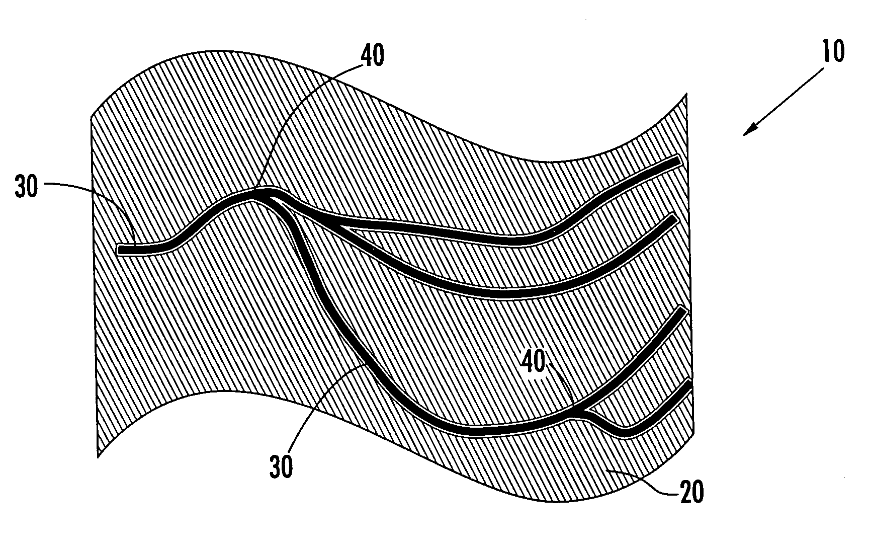
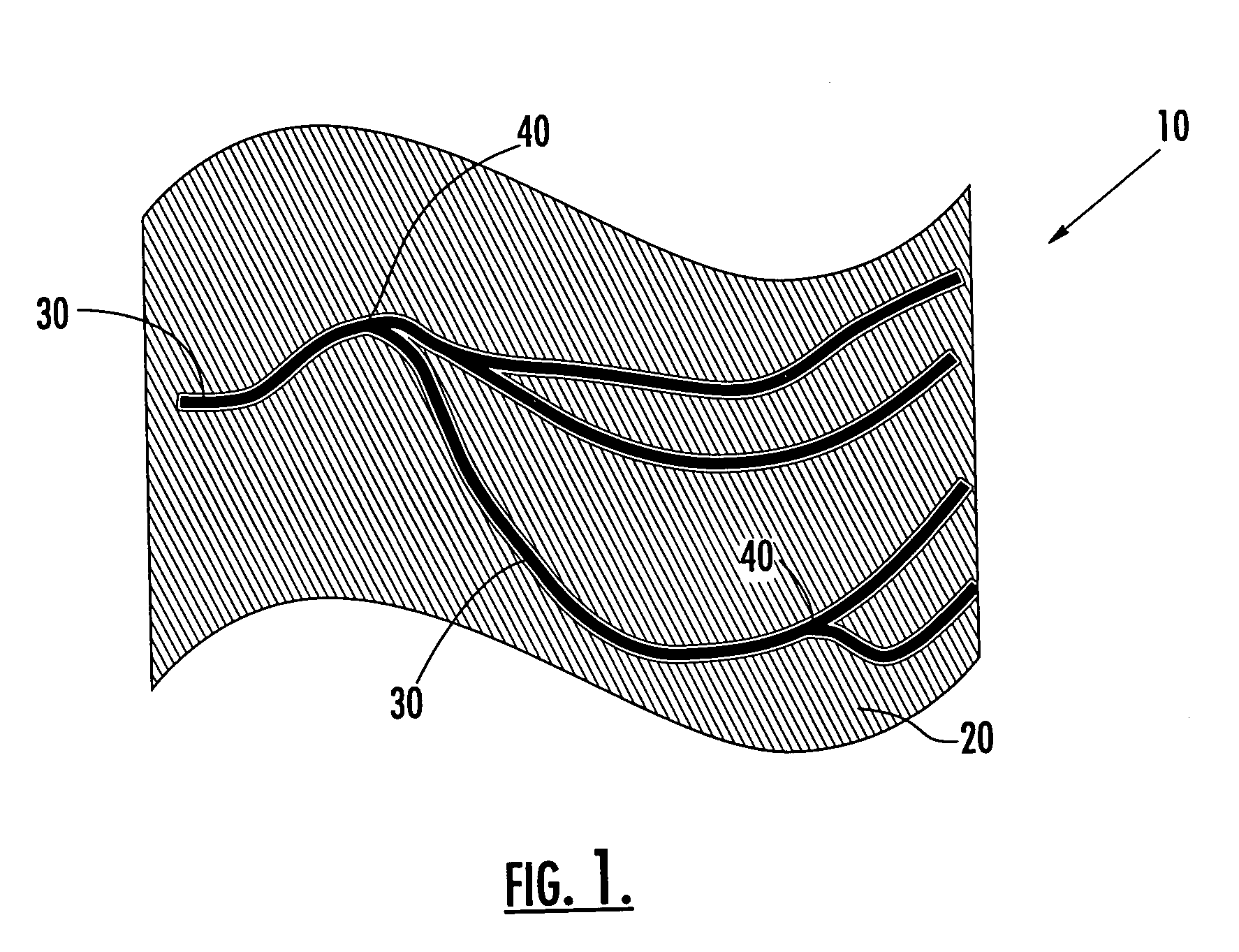
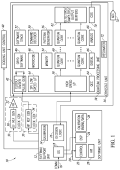
Integrated optical circuits
PatentInactiveUS7058245B2
Innovation
- The development of sol-gel based optical components and systems that utilize flexible polymeric substrates and low-temperature processing techniques to fabricate optical waveguides with rare earth ion doping and Bragg grating structures, enabling efficient integration of optical sources, detectors, and waveguides on a single substrate.
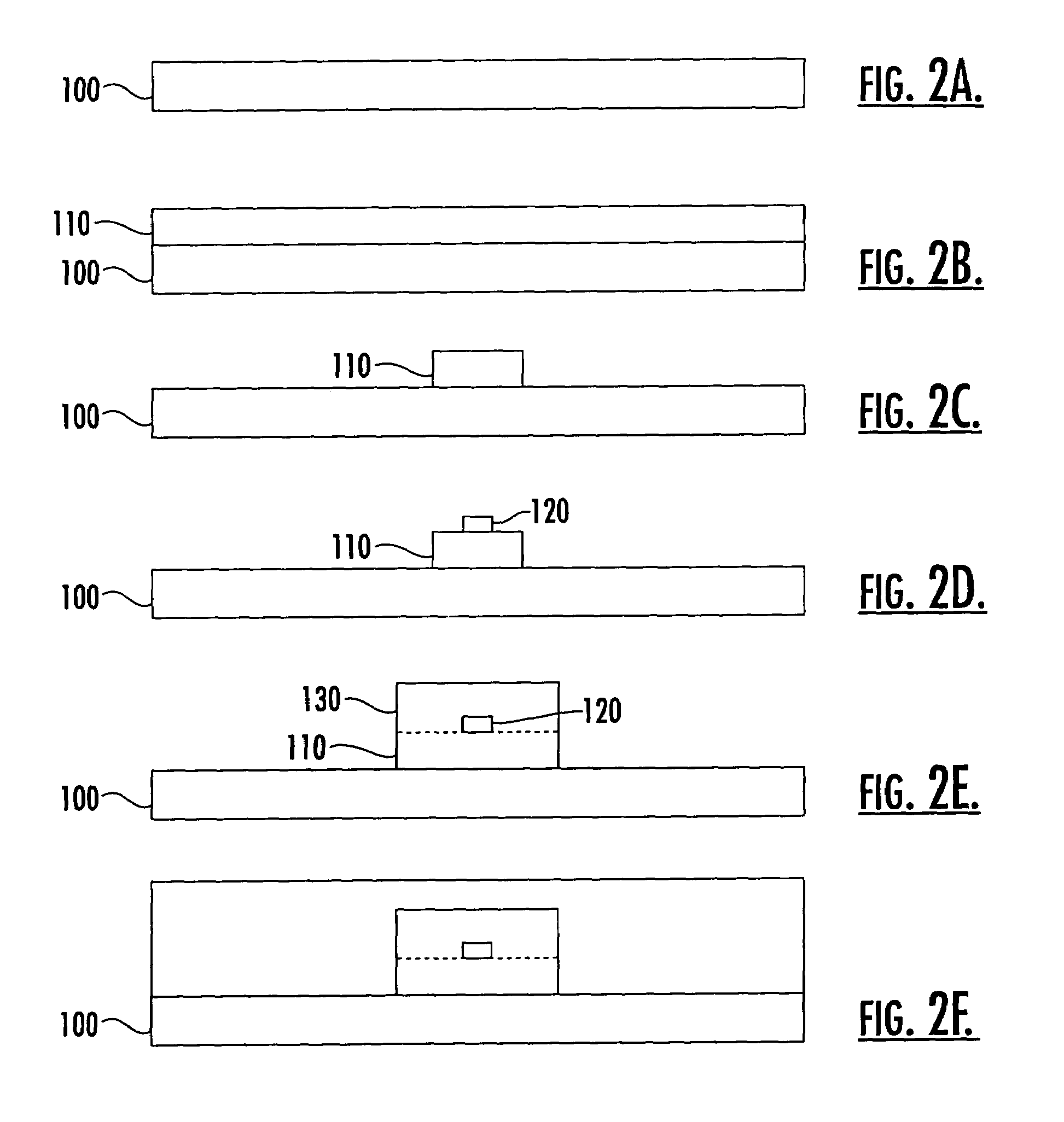
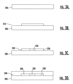
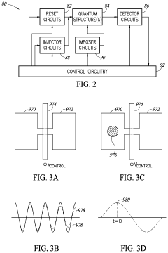
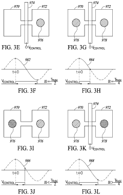
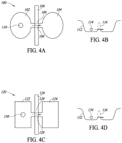
Quantum structures using aperture channel tunneling through depletion region
PatentActiveUS11450760B2
Innovation
- Semiconductor-based planar and 3D quantum structures utilizing tunneling through an oxide layer or local depleted wells to construct quantum dots and qubits, allowing controlled interaction and entanglement of particles, with control gates modulating tunneling between regions.
Materials Science Advancements for Quantum Circuits
Recent advancements in materials science have revolutionized the development of quantum circuits, particularly in addressing quantum tunneling scalability challenges in integrated optical circuits. Traditional materials like silicon and gallium arsenide have reached their physical limitations in supporting quantum operations at scale, necessitating exploration of novel material platforms.
Topological insulators represent a significant breakthrough, offering unique surface states that maintain quantum coherence even in the presence of environmental noise. Materials such as bismuth selenide (Bi₂Se₃) and bismuth telluride (Bi₂Te₃) demonstrate remarkable quantum tunneling properties while providing protection against decoherence, a critical factor in scaling quantum operations.
Two-dimensional materials, particularly transition metal dichalcogenides (TMDs) like MoS₂ and WSe₂, have emerged as promising candidates for quantum circuit integration. Their atomically thin nature facilitates precise control over quantum states, while their bandgap tunability enables optimization for specific quantum tunneling requirements. Recent experiments have demonstrated quantum tunneling efficiency improvements of up to 40% when incorporating these materials into integrated optical circuits.
Engineered metamaterials represent another frontier, with structures designed at the nanoscale to manipulate quantum tunneling phenomena. Hyperbolic metamaterials, composed of alternating metallic and dielectric layers, have demonstrated the ability to enhance photon-mediated tunneling processes by creating highly confined electromagnetic modes that strengthen light-matter interactions at quantum interfaces.
Superconducting materials continue to evolve, with recent developments in high-temperature superconductors like yttrium barium copper oxide (YBCO) and iron-based superconductors enabling quantum tunneling operations at more accessible temperature ranges. These materials significantly reduce cooling requirements, addressing a major scalability constraint in quantum circuit deployment.
Hybrid material systems combining different material classes have shown particular promise. For instance, integrating topological insulators with superconducting films creates unique interfaces where Majorana fermions can be generated and manipulated, offering new approaches to quantum information processing with inherent error correction properties.
Manufacturing advances have kept pace with material innovations, with atomic layer deposition and molecular beam epitaxy techniques now capable of creating atomically precise heterostructures. These fabrication capabilities are essential for translating theoretical material advantages into practical quantum circuit implementations that can scale beyond current limitations.
Quantum Computing Integration Opportunities
The integration of quantum computing with existing technological infrastructure presents unprecedented opportunities for advancement across multiple sectors. As quantum technologies mature, particularly in the realm of integrated optical circuits with enhanced quantum tunneling capabilities, we are witnessing the emergence of hybrid systems that leverage both classical and quantum computational paradigms.
The financial sector stands to benefit significantly from quantum computing integration. Quantum algorithms for portfolio optimization, risk assessment, and fraud detection could revolutionize financial services by processing complex market simulations at speeds unattainable by classical systems. Early adoption strategies are already being formulated by major financial institutions seeking competitive advantages through quantum-enhanced analytics.
Healthcare and pharmaceutical research represent another frontier for quantum integration. Drug discovery processes that currently require years of computational modeling could be accelerated dramatically through quantum simulation of molecular interactions. The ability to scale quantum tunneling in integrated circuits directly impacts the feasibility of these applications, potentially reducing development timelines and costs for life-saving medications.
Telecommunications infrastructure presents a natural integration point for quantum technologies. Quantum key distribution (QKD) systems are becoming increasingly viable for commercial deployment as quantum tunneling scalability improves. The security implications are profound, offering a pathway to communication networks theoretically immune to computational attacks, including those from future quantum computers themselves.
Manufacturing and logistics operations stand to benefit from quantum optimization algorithms that could transform supply chain management. Complex routing problems, inventory optimization, and demand forecasting could all be enhanced through quantum-classical hybrid approaches, with quantum processors handling specific computational bottlenecks while classical systems manage broader operational tasks.
Energy sector applications include grid optimization, materials science for battery development, and fusion energy research. Quantum simulations of complex molecular and atomic interactions could accelerate the discovery of novel materials with enhanced energy storage capabilities or superconducting properties at higher temperatures.
The defense and aerospace industries are exploring quantum sensing applications that leverage tunneling effects for unprecedented measurement precision. Navigation systems that operate independently of GPS, ultra-sensitive gravitational detectors, and advanced radar technologies all represent potential integration opportunities as quantum tunneling scalability improves in integrated optical circuits.
These integration opportunities collectively represent a transformative potential that extends far beyond the computing sector itself, potentially catalyzing innovation across the entire technological landscape as quantum capabilities become more accessible and reliable.
Unlock deeper insights with Patsnap Eureka Quick Research — get a full tech report to explore trends and direct your research. Try now!
Generate Your Research Report Instantly with AI Agent
Supercharge your innovation with Patsnap Eureka AI Agent Platform!