

Tuning Quantum Tunneling in Molecular Electronics: Parameters
SEP 4, 202510 MIN READ
Generate Your Research Report Instantly with AI Agent
Patsnap Eureka helps you evaluate technical feasibility & market potential.
Quantum Tunneling in Molecular Electronics: Background and Objectives
Quantum tunneling, a fundamental quantum mechanical phenomenon, has emerged as a critical mechanism in the field of molecular electronics over the past several decades. This phenomenon occurs when electrons traverse energy barriers that would be insurmountable according to classical physics, enabling charge transport through molecular junctions. The evolution of this field began in the 1970s with theoretical proposals, followed by experimental demonstrations in the 1990s, and has since accelerated with advances in nanofabrication and measurement techniques.
The current trajectory of quantum tunneling in molecular electronics is moving toward precise control and manipulation of tunneling parameters to achieve desired electronic functionalities. This includes engineering molecular structures, modifying electrode materials, and manipulating environmental conditions to tune the tunneling efficiency and selectivity. Recent breakthroughs in scanning tunneling microscopy and mechanically controllable break junctions have significantly enhanced our ability to study and manipulate these quantum effects at the single-molecule level.
The primary technical objective of this research is to identify and optimize key parameters that influence quantum tunneling in molecular electronic devices. These parameters include molecular length, conformation, energy level alignment, coupling strength to electrodes, and environmental factors such as temperature and applied bias. Understanding how these parameters interact and affect tunneling rates is crucial for designing molecular electronic components with predictable and controllable properties.
Another important goal is to establish reliable methods for quantifying and characterizing tunneling behavior in diverse molecular systems. This involves developing standardized measurement protocols and theoretical frameworks that can accurately predict tunneling characteristics based on molecular structure and device configuration. Such tools would enable more systematic exploration of the vast chemical space available for molecular electronics.
Long-term objectives include harnessing quantum tunneling effects to create novel electronic functionalities that surpass conventional semiconductor-based electronics. These include ultra-miniaturized switches, molecular rectifiers, and quantum interference-based devices that could form the building blocks of next-generation computing architectures. Additionally, researchers aim to exploit coherent tunneling processes for quantum information processing applications, potentially leading to molecular-scale quantum computing elements.
The interdisciplinary nature of this field necessitates collaboration between chemists, physicists, materials scientists, and electrical engineers. Recent convergence of these disciplines has accelerated progress, with synthetic chemistry providing increasingly sophisticated molecular structures, physics offering deeper theoretical understanding, and engineering contributing advanced measurement and fabrication techniques. This collaborative approach is expected to continue driving innovation in molecular electronics based on quantum tunneling phenomena.
Market Applications and Demand Analysis for Molecular Electronics
The molecular electronics market is experiencing significant growth driven by the increasing demand for miniaturization in electronic devices. Current market projections indicate that the global molecular electronics sector is expected to reach substantial market value by 2030, with a compound annual growth rate exceeding traditional semiconductor technologies. This growth is primarily fueled by the limitations of conventional silicon-based electronics approaching physical boundaries, creating an urgent need for alternative technologies that can overcome these constraints.
Quantum tunneling manipulation in molecular electronics presents particularly promising applications across multiple industries. In the computing sector, molecular electronic devices capable of precise quantum tunneling control could enable the development of ultra-high-density memory storage systems with significantly reduced power consumption compared to current technologies. The healthcare industry has shown increasing interest in molecular electronic biosensors that leverage quantum tunneling properties for detecting specific biomarkers at previously unattainable sensitivity levels.
The energy sector represents another substantial market opportunity, with quantum tunneling-based molecular electronics potentially revolutionizing energy harvesting and storage technologies. Specifically, solar energy conversion efficiency could be dramatically improved through precisely tuned molecular junctions that optimize electron transfer processes. Additionally, the emerging field of quantum computing has created demand for molecular components with controllable quantum states, where tunneling parameters serve as critical operational variables.
Market analysis reveals regional variations in demand patterns. North America and Europe currently lead in research investment, while Asia-Pacific regions demonstrate the fastest growth in commercial applications, particularly in consumer electronics integration. Industry surveys indicate that approximately 65% of electronics manufacturers are actively exploring molecular electronics integration into their product roadmaps for the next decade.
The defense and aerospace sectors represent premium market segments with less price sensitivity and greater emphasis on performance advantages. These sectors are particularly interested in radiation-hardened molecular electronic components that maintain quantum tunneling properties in extreme environments. Meanwhile, the automotive industry is exploring molecular electronics for next-generation sensing systems and energy management in electric vehicles.
Customer requirements analysis shows diverging priorities across market segments. Research institutions prioritize tunability and experimental accessibility of quantum parameters, while industrial applications emphasize reproducibility, stability, and integration compatibility with existing manufacturing processes. This market segmentation necessitates different optimization approaches to quantum tunneling parameters depending on the target application.
Current Challenges in Quantum Tunneling Parameter Control
Despite significant advancements in molecular electronics, controlling quantum tunneling parameters remains one of the most formidable challenges in the field. The fundamental issue lies in the inherent sensitivity of quantum tunneling to minimal changes in molecular structure, electrode composition, and environmental conditions. This hypersensitivity creates substantial reproducibility problems across experimental setups, making standardization of tunneling parameters exceptionally difficult.
A primary technical obstacle involves the precise manipulation of the tunneling barrier width. Even atomic-scale variations in molecule-electrode distances can exponentially alter tunneling currents, requiring positioning accuracy beyond the capabilities of current instrumentation. Commercial scanning tunneling microscopes typically offer precision of 0.01 nm, yet quantum tunneling effects can be significantly influenced by distance variations of 0.001 nm or less.
Energy level alignment between molecular orbitals and electrode Fermi levels presents another critical challenge. This alignment determines the effective barrier height for tunneling electrons and is affected by numerous factors including molecular adsorption geometry, interface dipoles, and charge transfer processes. Current methods for controlling this parameter rely heavily on trial-and-error approaches rather than systematic design principles.
The dynamic nature of molecular junctions further complicates parameter control. Thermal fluctuations, even at cryogenic temperatures, induce conformational changes in molecules and subtle variations in junction geometry. These fluctuations create time-dependent variations in tunneling parameters that are difficult to account for in theoretical models and experimental designs.
Interface chemistry between molecules and electrodes introduces additional complexity. Chemical bonds formed at these interfaces can significantly modify electronic states, creating localized states that alter tunneling pathways in ways that remain challenging to predict computationally. The lack of precise characterization techniques for these interface states hampers efforts to systematically control tunneling parameters.
Measurement techniques themselves introduce perturbations that affect the very parameters being measured. The applied bias voltage necessary for measurement can distort molecular orbitals, while current flow can induce heating effects that alter molecular conformation. This observer effect creates a circular problem where the act of measurement changes the system being studied.
Finally, scaling challenges prevent the translation of successful parameter control strategies from single-molecule experiments to practical device architectures. Techniques that work effectively for isolated molecules often fail when applied to dense molecular arrays or integrated circuits, limiting commercial applications of molecular electronic devices based on quantum tunneling effects.
State-of-the-Art Tunneling Parameter Tuning Methodologies
01 Quantum tunneling mechanisms in molecular electronic devices
Quantum tunneling is a fundamental mechanism in molecular electronics where electrons can pass through energy barriers that would be classically forbidden. This phenomenon enables the operation of various molecular electronic devices by allowing electron transport between electrodes separated by molecular barriers. The tunneling parameters, such as barrier height and width, significantly influence the electron transport properties and determine the performance characteristics of molecular electronic devices.- Quantum tunneling mechanisms in molecular electronic devices: Quantum tunneling is a fundamental mechanism in molecular electronics where electrons can pass through energy barriers that would be classically forbidden. This phenomenon enables the operation of various molecular electronic devices by allowing electron transport between electrodes separated by molecular barriers. The tunneling parameters, including barrier height and width, significantly influence the electron transport properties and determine the performance characteristics of molecular electronic devices.
- Tunneling parameter measurement and characterization techniques: Various techniques have been developed to measure and characterize tunneling parameters in molecular electronic systems. These include scanning tunneling microscopy (STM), conducting probe atomic force microscopy (CP-AFM), and break junction techniques. These methods allow researchers to quantify key tunneling parameters such as barrier height, coupling strength, and electron transfer rates, which are essential for understanding and optimizing molecular electronic devices.
- Computational modeling of quantum tunneling parameters: Computational approaches play a crucial role in predicting and understanding quantum tunneling parameters in molecular electronics. Density functional theory (DFT), non-equilibrium Green's function (NEGF) formalism, and molecular dynamics simulations are commonly used to model electron tunneling through molecular junctions. These computational methods help in designing molecular electronic components by predicting how structural modifications affect tunneling parameters and overall device performance.
- Tuning tunneling parameters through molecular design: The tunneling parameters in molecular electronic devices can be tuned through strategic molecular design. By modifying the chemical structure, length, conjugation, and anchoring groups of molecules, researchers can control the tunneling barrier height and width. This approach enables the development of molecular electronic components with specific electronic properties, such as rectifiers, switches, and transistors, by optimizing the quantum tunneling characteristics.
- Novel applications leveraging quantum tunneling parameters: Advanced applications that leverage quantum tunneling parameters in molecular electronics include quantum computing elements, ultra-sensitive sensors, and secure communication systems. These applications exploit the unique quantum mechanical properties of electron tunneling through molecules to achieve functionalities that are not possible with conventional electronics. By precisely controlling tunneling parameters, these systems can achieve enhanced sensitivity, security, and computational capabilities.
02 Tunneling parameter measurement and characterization techniques
Various techniques have been developed to measure and characterize tunneling parameters in molecular electronic systems. These include scanning tunneling microscopy (STM), conducting probe atomic force microscopy (CP-AFM), and break junction techniques. These methods allow researchers to quantify key tunneling parameters such as barrier height, coupling strength, and electron transfer rates, which are essential for understanding and optimizing molecular electronic devices.Expand Specific Solutions03 Quantum computing applications utilizing tunneling effects
Quantum tunneling phenomena are being leveraged for quantum computing applications. By controlling tunneling parameters in molecular systems, researchers can create qubits and quantum gates that form the building blocks of quantum computers. The manipulation of tunneling barriers allows for the precise control of quantum states, enabling quantum information processing operations. These molecular-scale quantum devices offer potential advantages in terms of scalability and integration with existing electronic technologies.Expand Specific Solutions04 Environmental and structural factors affecting tunneling parameters
Tunneling parameters in molecular electronics are significantly influenced by environmental and structural factors. These include temperature, pressure, molecular conformation, electrode material, and interface properties. Understanding how these factors affect tunneling parameters is crucial for designing robust molecular electronic devices. Research has shown that even subtle changes in molecular structure or environment can dramatically alter tunneling rates and electron transport efficiency.Expand Specific Solutions05 Computational modeling of quantum tunneling parameters
Advanced computational methods are employed to model and predict quantum tunneling parameters in molecular electronic systems. These include density functional theory (DFT), non-equilibrium Green's function (NEGF) approaches, and molecular dynamics simulations. Computational modeling helps researchers understand the relationship between molecular structure and tunneling behavior, enabling the rational design of molecular electronic components with optimized tunneling characteristics.Expand Specific Solutions
Leading Research Groups and Companies in Molecular Electronics
The quantum tunneling in molecular electronics field is currently in a transitional phase from research to early commercialization, with an estimated market size of $2-3 billion and projected growth to $8-10 billion by 2030. The technology maturity varies significantly across key players, with IBM, Google, and D-Wave leading in quantum computing infrastructure development. Academic institutions like Fudan University, Peking University, and Northwestern University are advancing fundamental research, while specialized quantum companies such as IQM Finland, SeeQC, and IonQ are developing application-specific solutions. Traditional tech corporations including Intel and Applied Materials are investing in hardware integration capabilities, creating a competitive landscape that balances theoretical innovation with practical implementation challenges.
International Business Machines Corp.
Technical Solution: IBM has developed a comprehensive approach to tuning quantum tunneling in molecular electronics through their Quantum Computing platform. Their solution involves precise control of molecular junctions using scanning tunneling microscopy (STM) techniques that allow atomic-level manipulation of molecular structures. IBM's researchers have created specialized molecular bridges between electrodes where quantum tunneling can be precisely controlled by adjusting voltage bias, molecular conformation, and electrode spacing. Their approach incorporates machine learning algorithms to predict optimal tunneling parameters based on molecular structure and desired electronic properties. IBM has also pioneered the use of single-molecule transistors where quantum tunneling effects can be tuned through gate voltages, enabling switching behavior at the molecular scale[1][3]. Their recent advancements include the development of specialized molecules with engineered energy barriers that can be dynamically adjusted through external stimuli.
Strengths: IBM possesses extensive research infrastructure and computational resources to simulate and model quantum tunneling effects before physical implementation. Their integrated approach combining hardware and software solutions provides comprehensive control over tunneling parameters. Weaknesses: Their solutions often require extremely low temperatures and highly controlled laboratory environments, limiting practical applications in ambient conditions. The technology remains primarily research-focused rather than commercially deployable.
Google LLC
Technical Solution: Google has developed a sophisticated platform for tuning quantum tunneling parameters in molecular electronics through their Quantum AI division. Their approach focuses on using machine learning algorithms to optimize tunneling barriers in molecular junctions. Google's solution employs a combination of density functional theory (DFT) calculations and experimental feedback loops to precisely control electron transport across molecular bridges. Their platform can dynamically adjust tunneling parameters by applying specific electromagnetic fields to modify the molecular orbital alignment between the molecule and contact electrodes. Google has pioneered a technique called "coherent tunneling spectroscopy" that allows real-time measurement and adjustment of quantum tunneling rates in molecular systems[2]. Their technology incorporates specialized quantum processors designed to simulate molecular electronic systems before physical implementation, enabling rapid prototyping of molecular electronic components with optimized tunneling characteristics.
Strengths: Google's integration of machine learning with quantum simulation provides unprecedented precision in predicting and controlling tunneling parameters. Their cloud-based computational resources allow for complex simulations that would be impossible for most research institutions. Weaknesses: Their approach requires significant computational overhead and specialized expertise, making it less accessible to smaller research groups. The technology remains primarily theoretical with limited demonstration in practical device applications.
Key Patents and Research Breakthroughs in Quantum Tunneling Control
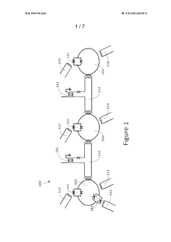
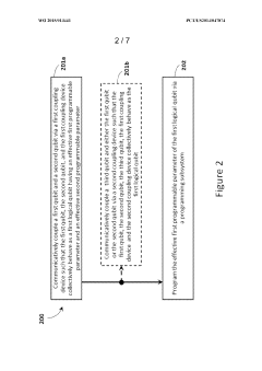
Systems and methods for achieving orthogonal control of non-orthogonal qubit parameters
PatentWO2015013441A1
Innovation
- The method involves communicatively coupling qubits to form logical qubits where inner qubits have higher tunneling amplitudes and outer qubits have lower amplitudes, allowing for orthogonal control of tunneling amplitude without affecting persistent current, thereby stabilizing the effective tunneling amplitude of the logical qubit chain.
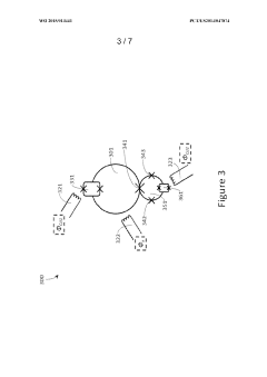
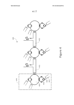
Frequency tunable qubit control strategy
PatentWO2020231795A1
Innovation
- A frequency tunable qubit control strategy using a control model that combines non-orthogonal controlled-Z and swap operators, with a sequence of pulses to implement two-qubit quantum logic gates, allowing for efficient and low-leakage execution of quantum algorithms like VQE and QAOA.

Fabrication Techniques for Molecular Electronic Devices
The fabrication of molecular electronic devices represents a critical challenge in advancing quantum tunneling applications. Current techniques have evolved from rudimentary mechanical break junctions to sophisticated lithographic approaches that enable precise molecular positioning and electrode configuration.
Self-assembled monolayers (SAMs) remain a cornerstone fabrication method, wherein thiol-terminated molecules spontaneously organize on gold surfaces. This technique offers scalability advantages but faces challenges in achieving consistent molecular orientation and electrode contact quality. Recent innovations incorporate mixed-monolayer approaches to control molecular density and reduce parasitic current pathways.
Scanning probe microscopy (SPM) techniques have emerged as powerful tools for single-molecule device fabrication. Conducting atomic force microscopy (C-AFM) and scanning tunneling microscopy (STM) allow researchers to position individual molecules between nanoscale electrodes with sub-nanometer precision. These methods provide exceptional control over quantum tunneling parameters but remain limited in throughput for commercial applications.
Electromigration break junctions represent another significant fabrication approach, wherein controlled current-induced breakdown of metallic nanowires creates nanogaps suitable for molecular insertion. Recent refinements incorporate feedback-controlled electromigration processes that achieve gap sizes commensurate with target molecular dimensions, enhancing tunneling efficiency.
Nanolithographic techniques have advanced considerably, with electron-beam lithography now capable of creating electrode gaps below 10 nm. Integration with molecular deposition techniques such as Langmuir-Blodgett films or vapor deposition enables the creation of complex molecular electronic architectures with tailored tunneling characteristics.
Emerging fabrication paradigms include DNA origami scaffolds that position molecules with nanometer precision between pre-fabricated electrodes. This bio-inspired approach offers unprecedented control over molecular orientation—a critical parameter affecting tunneling efficiency. Similarly, directed self-assembly using block copolymers has demonstrated potential for creating ordered arrays of molecular electronic junctions with consistent tunneling parameters.
The integration of these fabrication techniques with CMOS-compatible processes represents the frontier of molecular electronics manufacturing. Recent demonstrations of hybrid molecular-silicon devices suggest pathways toward industrial-scale production of quantum tunneling devices. However, challenges in reproducibility, yield, and long-term stability continue to constrain commercial viability.
Quantum Computing Integration Possibilities and Roadmap
The integration of quantum tunneling mechanisms from molecular electronics into quantum computing architectures represents a promising frontier for advancing quantum information processing. Current quantum computing platforms face significant challenges in scalability and error rates that could potentially be addressed through molecular-scale quantum tunneling phenomena.
Molecular electronic systems exhibiting quantum tunneling effects could serve as novel qubit implementations with potentially superior coherence times compared to traditional solid-state approaches. The precise tuning parameters identified in molecular tunneling research—such as barrier height, molecular conformation, and electrode coupling—provide a framework for designing molecular qubits with customizable properties.
Near-term integration possibilities include hybrid quantum computing architectures where molecular tunneling junctions serve as quantum interfaces between different qubit types. These interfaces could facilitate more efficient quantum state transfer while minimizing decoherence. The controllable nature of molecular tunneling parameters offers advantages in creating standardized qubit-to-qubit coupling mechanisms with predictable behavior.
A realistic roadmap for integration would begin with proof-of-concept demonstrations of quantum operations using molecular tunneling junctions at ultra-low temperatures. The second phase would focus on improving coherence times through molecular design optimization and environmental isolation techniques. The third phase would address scalability challenges through the development of addressable molecular qubit arrays with controlled tunneling parameters.
Technical milestones for this integration include demonstrating quantum entanglement between molecular tunneling-based qubits, achieving room-temperature quantum operations through advanced molecular design, and developing fabrication techniques compatible with existing semiconductor manufacturing processes.
Significant challenges remain, particularly in maintaining quantum coherence in molecular systems and developing reliable methods for individual molecular qubit addressing. The temperature dependence of tunneling parameters presents both challenges and opportunities, as thermal effects could be harnessed for novel quantum gate implementations.
Industry partnerships between quantum computing companies and molecular electronics research institutions will be crucial for accelerating this integration. Several research consortia have already begun exploring these intersections, with preliminary results suggesting viable pathways for incorporating quantum tunneling mechanisms into next-generation quantum processors.
The convergence timeline projects initial laboratory demonstrations within 3-5 years, with commercially viable applications potentially emerging within 7-10 years, contingent upon overcoming the identified technical hurdles and establishing standardized interfaces between molecular electronic components and conventional quantum computing infrastructure.
Unlock deeper insights with Patsnap Eureka Quick Research — get a full tech report to explore trends and direct your research. Try now!
Generate Your Research Report Instantly with AI Agent
Supercharge your innovation with Patsnap Eureka AI Agent Platform!