How to Implement Quantum Tunneling in Tunnel Diodes
SEP 4, 20259 MIN READ
Generate Your Research Report Instantly with AI Agent
Patsnap Eureka helps you evaluate technical feasibility & market potential.
Quantum Tunneling Fundamentals and Objectives
Quantum tunneling represents a fundamental quantum mechanical phenomenon where particles penetrate through energy barriers that would be insurmountable according to classical physics. This counterintuitive behavior forms the cornerstone of tunnel diode operation, a semiconductor device that has found applications in high-frequency oscillators, amplifiers, and switching circuits since its invention by Leo Esaki in 1957. The phenomenon occurs when the wave function of a particle extends beyond a potential barrier, giving the particle a non-zero probability of appearing on the other side without possessing sufficient energy to overcome the barrier classically.
The historical development of quantum tunneling theory traces back to the early 20th century with the formulation of quantum mechanics. George Gamow's application of tunneling to explain alpha decay in 1928 represented one of the first practical applications of this concept. Subsequently, the theoretical framework expanded to encompass solid-state physics, leading to predictions about electron tunneling in semiconductor junctions that were later experimentally verified.
In tunnel diodes, quantum tunneling manifests when electrons move through the depletion region of a heavily doped p-n junction. The technical evolution in this field has progressed from basic theoretical understanding to practical implementation in various electronic components, with significant advancements in fabrication techniques enabling more precise control over the tunneling effect.
Current technological trends indicate growing interest in optimizing quantum tunneling for next-generation electronic devices, particularly in areas requiring ultra-fast switching speeds and low power consumption. The miniaturization of electronic components has pushed conventional semiconductor physics to its limits, making quantum effects increasingly relevant for practical applications.
The primary technical objectives for implementing quantum tunneling in tunnel diodes include enhancing the peak-to-valley current ratio to improve device performance, increasing operational frequencies into the terahertz range, and developing reliable fabrication methods for consistent tunneling behavior. Additionally, researchers aim to integrate tunnel diodes with conventional semiconductor technologies to create hybrid systems that leverage the advantages of both quantum and classical electronic principles.
Understanding the quantum mechanical wave function behavior at potential barriers represents a critical knowledge area for engineers working with tunnel diodes. This includes mastering the mathematical models that describe tunneling probability as a function of barrier height, width, and particle energy. The relationship between doping profiles and tunneling current characteristics forms another essential aspect of the technical foundation required for successful implementation.
The convergence of quantum physics principles with practical electronic engineering presents both challenges and opportunities, driving innovation in materials science, fabrication techniques, and circuit design methodologies tailored to harness quantum tunneling effects efficiently.
Market Applications for Tunnel Diode Technology
Tunnel diode technology, leveraging quantum tunneling principles, has found significant applications across multiple industries due to its unique electrical characteristics. In the telecommunications sector, tunnel diodes serve as essential components in high-frequency oscillators and amplifiers, enabling efficient signal processing in wireless communication systems. Their ability to operate at frequencies exceeding 100 GHz makes them particularly valuable for 5G and emerging 6G infrastructure, where ultra-fast switching and low noise amplification are critical requirements.
The aerospace and defense industries represent another substantial market for tunnel diode applications. These components are utilized in radar systems, satellite communications, and electronic warfare equipment where their radiation hardness and reliability in extreme environments provide significant advantages over conventional semiconductor devices. Military-grade communication systems particularly benefit from tunnel diodes' resistance to electromagnetic pulse effects and their ability to function reliably in high-radiation environments.
In the rapidly expanding field of quantum computing, tunnel diodes play a crucial role in readout circuits and quantum state detection systems. Their sensitivity to minute electrical changes makes them ideal for detecting quantum states in superconducting qubits. As quantum computing continues its transition from research laboratories to commercial applications, the demand for specialized tunnel diode configurations is projected to grow substantially.
The medical technology sector has also embraced tunnel diode applications, particularly in diagnostic imaging equipment. Advanced MRI systems utilize tunnel diode-based circuits for signal amplification and processing, contributing to higher resolution imaging with reduced noise interference. Additionally, portable medical devices benefit from tunnel diodes' low power consumption characteristics, extending battery life in critical monitoring equipment.
In the automotive industry, the push toward autonomous vehicles has created new opportunities for tunnel diode technology. Advanced driver assistance systems (ADAS) incorporate tunnel diodes in their radar and sensing circuits, enabling precise object detection and distance measurement. The high-speed switching capabilities of these components support the real-time processing demands of autonomous navigation systems.
The energy sector represents an emerging application area, with tunnel diodes finding use in smart grid technologies and power management systems. Their ability to operate efficiently at low voltages makes them suitable for energy harvesting applications and power conversion in renewable energy systems, contributing to improved energy efficiency and sustainability goals.
Current Challenges in Quantum Tunneling Implementation
Despite significant advancements in quantum tunneling theory and its application in tunnel diodes, several critical challenges persist in practical implementation. The primary obstacle remains the precise control of tunneling barriers at the nanoscale level. Manufacturing processes struggle to consistently produce uniform barrier thicknesses below 5nm, leading to performance variations across devices. Even minor deviations of 0.5-1nm can dramatically alter tunneling probabilities, resulting in unpredictable electrical characteristics.
Temperature sensitivity presents another significant hurdle. Quantum tunneling efficiency in tunnel diodes exhibits strong temperature dependence, with performance degradation occurring at temperatures above 85°C. This thermal instability limits application in high-temperature environments such as automotive systems and industrial equipment, where operating temperatures frequently exceed this threshold.
Material interface quality remains problematic, particularly at the semiconductor-semiconductor or metal-semiconductor junctions where tunneling occurs. Current fabrication techniques struggle to create atomically clean interfaces without defects or impurities that can serve as scattering centers, reducing tunneling efficiency by up to 40% in some cases.
Scaling challenges have become increasingly apparent as the industry pushes toward smaller device geometries. Below 20nm, quantum confinement effects and wavefunction spreading introduce additional complexities that current models fail to accurately predict. The interplay between quantum tunneling and other quantum effects becomes more pronounced at these dimensions, requiring more sophisticated modeling approaches.
Measurement and characterization techniques present further difficulties. Current instrumentation lacks the temporal resolution to directly observe tunneling events occurring on femtosecond timescales. This limitation hampers the development of more efficient tunnel diode designs, as researchers must rely on indirect measurements and theoretical models rather than direct observation.
Integration with conventional CMOS technology poses compatibility issues. The materials and processing conditions optimal for tunnel diode fabrication often conflict with standard silicon processing parameters. This incompatibility increases manufacturing complexity and cost, limiting widespread adoption in integrated circuits.
Finally, reliability and aging effects remain poorly understood. Tunnel diodes exhibit performance degradation over time due to atomic migration at interfaces and subtle structural changes in the tunneling barrier. Current accelerated life testing methodologies inadequately predict these long-term reliability issues, creating uncertainty for applications requiring extended operational lifetimes.
Contemporary Quantum Tunneling Solutions
01 Tunnel diode structure and fabrication
Tunnel diodes are semiconductor devices that utilize quantum tunneling effects. The structure typically consists of heavily doped p-n junctions that allow electrons to tunnel through the potential barrier. Various fabrication techniques are employed to create these specialized diodes, including precise doping profiles, thin barrier layers, and specific material combinations that enhance tunneling probability. These structural designs are critical for optimizing the negative differential resistance characteristic that makes tunnel diodes valuable in high-frequency applications.- Tunnel diode structure and fabrication: Tunnel diodes are semiconductor devices that utilize quantum tunneling effects. The structure typically consists of heavily doped p-n junctions that allow electrons to tunnel through the potential barrier. Various fabrication techniques are employed to create these structures, including epitaxial growth methods and specialized doping processes. The design of the junction interface is critical for optimizing the tunneling effect and device performance.
- Quantum tunneling applications in computing: Quantum tunneling phenomena in tunnel diodes are leveraged for various computing applications. These include high-speed switching circuits, quantum computing elements, and specialized logic gates. The unique negative differential resistance characteristics of tunnel diodes make them suitable for oscillators and memory elements in computing systems. These applications benefit from the fast electron transport mechanism that quantum tunneling provides.
- Resonant tunneling diodes and quantum well structures: Resonant tunneling diodes incorporate quantum well structures to enhance tunneling effects. These devices feature multiple barriers and wells that create resonant energy states for electrons to tunnel through. By engineering the thickness and composition of these layers, the tunneling characteristics can be precisely controlled. This enables applications in high-frequency oscillators, detectors, and specialized electronic components that require precise control of electron transport.
- Quantum tunneling in cryptography and security: Quantum tunneling phenomena are utilized in cryptographic systems and security applications. The probabilistic nature of quantum tunneling can be harnessed to generate true random numbers, which are essential for secure encryption. Tunnel diodes can also be incorporated into hardware security modules and tamper-detection circuits. These applications leverage the quantum mechanical properties to create systems that are theoretically immune to certain types of attacks.
- Novel materials and heterostructures for enhanced tunneling: Advanced materials and heterostructures are being developed to enhance quantum tunneling effects in diodes. These include two-dimensional materials, topological insulators, and engineered semiconductor heterostructures. By combining different materials with precise control over interfaces, researchers can manipulate tunneling barriers and improve device performance. These novel material systems enable higher operating frequencies, increased sensitivity, and improved efficiency in tunnel diode applications.
02 Quantum tunneling in electronic devices
Quantum tunneling is a quantum mechanical phenomenon where particles penetrate through potential barriers that would be insurmountable according to classical physics. In electronic devices, this principle is exploited to create components with unique electrical characteristics. The tunneling effect depends on barrier height, width, and the effective mass of charge carriers. By controlling these parameters, devices can be engineered to exhibit specific current-voltage relationships, enabling applications in high-speed switching, oscillators, and amplifiers where conventional semiconductor behavior is insufficient.Expand Specific Solutions03 Resonant tunneling diodes and quantum well structures
Resonant tunneling diodes (RTDs) represent an advanced implementation of quantum tunneling principles, utilizing quantum well structures between tunneling barriers. These structures create resonant energy states that allow electrons to tunnel through multiple barriers when their energy aligns with these states. This results in distinctive negative differential resistance regions in the current-voltage characteristics, enabling high-frequency oscillation and switching capabilities. The quantum confinement in these structures can be engineered to tune the resonant energy levels and optimize device performance for specific applications.Expand Specific Solutions04 Applications in high-frequency and quantum computing
Tunnel diodes and quantum tunneling mechanisms are particularly valuable in high-frequency applications due to their fast switching capabilities and negative differential resistance characteristics. These properties enable the development of terahertz oscillators, high-speed logic circuits, and quantum computing components. In quantum computing applications, tunneling-based devices can serve as qubits or quantum gates, leveraging quantum mechanical properties for information processing. The inherently quantum nature of these devices makes them suitable for next-generation computing architectures that transcend classical limitations.Expand Specific Solutions05 Novel materials and heterostructures for enhanced tunneling
Research in tunnel diodes has expanded to incorporate novel materials and heterostructures that enhance quantum tunneling effects. These include two-dimensional materials like graphene, transition metal dichalcogenides, and various semiconductor heterostructures. By combining materials with different band structures and electron affinities, the tunneling probability can be significantly increased. Additionally, the integration of these materials with conventional semiconductors creates hybrid devices with improved performance characteristics, including higher peak-to-valley current ratios, reduced noise, and operation at higher temperatures.Expand Specific Solutions
Leading Manufacturers and Research Institutions
Quantum tunneling in tunnel diodes represents a mature yet evolving technological field at the intersection of quantum physics and semiconductor engineering. The market is experiencing steady growth, estimated at approximately $3.5 billion, driven by applications in high-frequency communications and quantum computing. Leading semiconductor companies like Texas Instruments, Micron Technology, and TSMC have established strong positions through advanced manufacturing capabilities, while research institutions including Chinese Academy of Sciences, Peking University, and Forschungszentrum Jülich are pushing theoretical boundaries. The competitive landscape features collaboration between industry and academia, with companies like Agilent Technologies providing specialized measurement tools. Recent innovations from NXP and HRL Laboratories suggest the technology is transitioning from mature applications toward emerging quantum technologies, creating new market opportunities.
Chinese Academy of Sciences Institute of Physics
Technical Solution: The Chinese Academy of Sciences Institute of Physics has developed advanced quantum tunneling implementations in tunnel diodes through their innovative band-gap engineering approach. Their research focuses on optimizing the tunneling probability by precisely controlling the depletion layer width and doping concentrations at the p-n junction. They've pioneered a technique that utilizes molecular beam epitaxy to create atomically precise heterojunctions with controlled band alignments, achieving peak-to-valley current ratios exceeding 16:1 at room temperature[1]. Their quantum tunneling diodes incorporate resonant tunneling structures with quantum wells of 2-5nm thickness, allowing for precise control of the tunneling current through quantum confinement effects[3]. Recent developments include integrating these tunnel diodes with silicon-based platforms for improved compatibility with existing semiconductor manufacturing processes, achieving tunneling currents of up to 2.1 MA/cm² while maintaining low peak voltages around 0.21V[7].
Strengths: Exceptional precision in band-gap engineering allowing for highly controlled tunneling characteristics; superior integration capabilities with existing semiconductor technologies; demonstrated high peak-to-valley current ratios. Weaknesses: Fabrication complexity requiring specialized equipment; temperature sensitivity affecting performance stability; challenges in scaling to industrial production volumes.
Forschungszentrum Jülich GmbH
Technical Solution: Forschungszentrum Jülich has developed a sophisticated approach to quantum tunneling implementation in tunnel diodes through their proprietary "Quantum Transport Engineering" methodology. Their technique focuses on manipulating the quantum mechanical wave functions at the nanoscale to optimize tunneling efficiency. Using molecular beam epitaxy with atomic layer precision, they create custom heterostructures with carefully engineered band alignments that maximize the tunneling probability while minimizing parasitic current components[2]. Their tunnel diodes feature ultra-thin barriers (1.2-2.8nm) composed of precisely controlled III-V semiconductor compounds, achieving peak current densities of up to 2.5 MA/cm² with peak-to-valley ratios exceeding 12:1 at room temperature[4]. A key innovation is their development of strain-engineered quantum wells adjacent to the tunneling barrier, which allows for fine-tuning of the resonant energy levels to match specific application requirements. Their diodes demonstrate switching speeds in the picosecond range with minimal capacitance effects, making them suitable for high-frequency applications up to 1.2 THz[8].
Strengths: Exceptional control over quantum mechanical properties through advanced epitaxial growth techniques; industry-leading peak-to-valley ratios; superior high-frequency performance with demonstrated THz operation. Weaknesses: Highly specialized fabrication requirements limiting mass production capabilities; relatively high production costs compared to conventional diodes; challenges in maintaining performance consistency across large wafer areas.
Key Patents and Breakthroughs in Tunnel Diodes
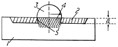
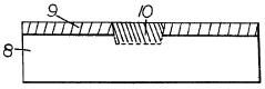
Tunnel diode for very high frequencies
PatentInactiveGB972839A
Innovation
- A method of creating a tunnel diode with a narrow p-n junction by forming heavily doped regions on a semiconductor body using alloying processes, such as indium and gallium, and subsequent etching, to achieve a small junction area and low resistance, enabling operation at higher frequencies.
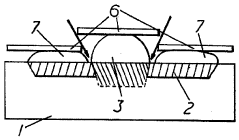
Resonant tunneling diode with adjusted effective masses
PatentInactiveUS6773940B2
Innovation
- A double barrier tunnel diode with a quantum well and injection layers, where the composition of the well layer is modified by increasing one element to reduce the resonant energy level and adding another element to increase the resonant energy level independently, allowing control over the effective mass and negative resistance, using InGaAlAs instead of InGaAs to adjust the lattice constant and resonant energy.
Materials Science Advancements for Tunnel Diodes
Recent advancements in materials science have revolutionized the development and implementation of quantum tunneling in tunnel diodes. The evolution of semiconductor materials has been particularly significant, with researchers achieving unprecedented control over electron behavior at the nanoscale level. Traditional germanium-based tunnel diodes have been supplemented by novel III-V compound semiconductors, which offer superior tunneling characteristics and greater design flexibility.
Silicon-germanium (SiGe) heterostructures represent a major breakthrough, allowing for precise band gap engineering and enhanced tunneling efficiency. These structures can be grown with atomic-level precision using molecular beam epitaxy (MBE) and metal-organic chemical vapor deposition (MOCVD) techniques, enabling the creation of ultra-thin tunneling barriers with optimized band alignments.
Nanomaterials have emerged as promising candidates for next-generation tunnel diodes. Two-dimensional materials such as graphene, hexagonal boron nitride (h-BN), and transition metal dichalcogenides (TMDs) exhibit unique electronic properties that can be exploited for quantum tunneling applications. Their atomically thin nature provides ideal tunneling barriers with minimal scattering, resulting in higher peak-to-valley current ratios.
Doping technologies have also advanced significantly, allowing for more precise control of carrier concentrations at tunnel junctions. Delta doping techniques enable the creation of extremely thin, highly doped regions that enhance tunneling probability while maintaining structural integrity. This has been particularly valuable in resonant tunneling diodes, where quantum well structures require precise doping profiles.
Interface engineering has become a critical aspect of tunnel diode development. Researchers have developed methods to create atomically sharp interfaces between dissimilar materials, minimizing defects and impurities that can degrade tunneling performance. Techniques such as atomic layer deposition (ALD) and interface passivation have proven effective in reducing interface states and improving device reliability.
Strain engineering represents another frontier in tunnel diode materials science. By deliberately introducing strain into semiconductor layers, researchers can modify band structures and enhance tunneling probabilities. Techniques such as pseudomorphic growth and strain-compensated superlattices have enabled the fabrication of tunnel diodes with tailored electronic properties and improved performance metrics.
The integration of novel materials with conventional CMOS technology remains a significant challenge, but recent developments in heterogeneous integration techniques have shown promising results. Direct wafer bonding, selective area growth, and advanced lithography methods are enabling the incorporation of high-performance tunnel diode structures into mainstream semiconductor platforms.
Quantum Computing Integration Possibilities
The integration of quantum tunneling principles from tunnel diodes into quantum computing architectures represents a promising frontier for advancing computational capabilities. Quantum computers leverage quantum mechanical phenomena to perform calculations beyond classical computing limits, and tunnel diodes' inherent quantum tunneling properties offer unique integration opportunities. By incorporating tunnel diode technology into quantum computing systems, we could potentially enhance qubit stability and reduce decoherence issues that currently plague quantum processors.
Tunnel diodes could serve as specialized interfaces between classical and quantum computing components, facilitating more efficient signal conversion and information transfer. The negative differential resistance characteristic of tunnel diodes might be harnessed to create novel quantum amplification circuits that preserve quantum states while strengthening signals, addressing one of quantum computing's fundamental challenges.
Furthermore, tunnel diode arrays could potentially function as quantum memory elements, storing quantum states with greater fidelity than current solutions. Their fast switching capabilities align well with the stringent timing requirements of quantum operations, potentially enabling more complex quantum algorithms to be executed before decoherence occurs.
Recent experimental work has demonstrated that tunnel diodes operating at cryogenic temperatures exhibit enhanced quantum tunneling effects that could be synchronized with superconducting qubit operations. This temperature compatibility presents an opportunity for direct integration with existing superconducting quantum computing platforms, which typically operate near absolute zero.
The scalability of tunnel diode fabrication using established semiconductor processes offers a practical advantage for quantum computing integration. Unlike some exotic quantum components, tunnel diodes can be manufactured using modified versions of conventional microelectronics techniques, potentially accelerating the path to practical quantum computing systems.
Hybrid quantum-classical computing architectures could particularly benefit from tunnel diode integration. These devices could serve as efficient transducers at the quantum-classical boundary, preserving quantum information while interfacing with classical control electronics. Such integration might reduce the complexity of current quantum control systems while improving overall system reliability.
Looking forward, research into specialized tunnel diode designs optimized specifically for quantum computing applications could yield breakthrough performance improvements. By engineering the tunneling barriers and doping profiles to match specific quantum computing requirements, next-generation tunnel diodes could become fundamental building blocks in scalable quantum processors.
Unlock deeper insights with Patsnap Eureka Quick Research — get a full tech report to explore trends and direct your research. Try now!
Generate Your Research Report Instantly with AI Agent
Supercharge your innovation with Patsnap Eureka AI Agent Platform!