Quantum Tunneling in Microfluidic Devices: Efficiency Factors
SEP 4, 202510 MIN READ
Generate Your Research Report Instantly with AI Agent
Patsnap Eureka helps you evaluate technical feasibility & market potential.
Quantum Tunneling Fundamentals and Research Objectives
Quantum tunneling represents a fundamental quantum mechanical phenomenon where particles penetrate through energy barriers that would be insurmountable according to classical physics. This counterintuitive behavior stems from the wave-particle duality described by quantum mechanics, where particles exhibit wavelike properties at the nanoscale. The historical development of quantum tunneling theory traces back to the early 20th century, with significant contributions from physicists like Friedrich Hund, George Gamow, and Ronald Gurney, who applied the concept to explain alpha decay in radioactive nuclei.
In recent decades, quantum tunneling has transitioned from a purely theoretical concept to a practical consideration in various technological applications, particularly in semiconductor devices and scanning tunneling microscopy. The emergence of microfluidic technology has created a novel intersection where quantum effects meet fluid dynamics at the microscale, opening unprecedented research avenues.
The integration of quantum tunneling principles with microfluidic devices represents an evolving technological frontier with significant potential for innovation. Current research indicates that quantum tunneling effects can influence electron transport mechanisms within microfluidic channels, potentially enhancing efficiency in various applications including biosensing, energy conversion, and chemical synthesis processes.
The technological trajectory suggests a convergence of quantum physics and microfluidics, driven by advances in nanofabrication techniques and quantum measurement methodologies. This convergence enables precise manipulation of quantum effects within controlled fluidic environments, potentially revolutionizing how we approach microscale chemical and biological processes.
Our research objectives focus on systematically investigating the efficiency factors that govern quantum tunneling phenomena in microfluidic architectures. Specifically, we aim to quantify how parameters such as barrier geometry, temperature fluctuations, and electromagnetic field variations affect tunneling probabilities within microfluidic channels. Additionally, we seek to develop predictive models that can accurately simulate quantum tunneling behavior under various operational conditions relevant to practical microfluidic applications.
The long-term technological goal encompasses the development of design principles for quantum-enhanced microfluidic devices that leverage tunneling effects to achieve superior performance metrics compared to conventional designs. This includes exploring how controlled quantum tunneling might enable more sensitive detection mechanisms, more efficient catalytic processes, or novel separation techniques within microfluidic platforms.
Furthermore, we aim to establish a comprehensive framework for evaluating quantum tunneling efficiency in diverse microfluidic configurations, providing the scientific community with standardized methodologies for characterizing and optimizing these quantum effects in practical applications.
Market Applications for Quantum-Enhanced Microfluidics
Quantum-enhanced microfluidic technologies are poised to revolutionize multiple industries by leveraging quantum tunneling effects to improve efficiency and precision in microscale fluid handling. The healthcare sector represents the most promising immediate market application, with quantum-enhanced lab-on-chip devices enabling unprecedented sensitivity in diagnostic testing. These systems can detect biomarkers at concentrations previously unattainable, potentially transforming early disease detection for conditions like cancer and neurodegenerative diseases.
Pharmaceutical research and development stands to benefit significantly from quantum-enhanced microfluidics through dramatically improved drug discovery processes. The technology enables more precise manipulation of minute sample volumes, accelerating high-throughput screening while reducing reagent consumption. Industry analysts project this could reduce early-stage drug development timelines by up to 30% and substantially decrease associated costs.
Environmental monitoring represents another substantial market opportunity. Quantum-tunneling microfluidic sensors deployed in water quality monitoring systems can detect contaminants at parts-per-trillion levels, far exceeding conventional detection methods. This capability addresses growing regulatory and public demands for more stringent environmental protection measures across industrial and municipal sectors.
The semiconductor manufacturing industry is exploring quantum-enhanced microfluidics for next-generation lithography processes. The precise control of fluid dynamics at quantum scales could enable more efficient etching processes and novel cooling solutions for increasingly dense chip architectures. Early adopters in this space are primarily focused on addressing thermal management challenges in advanced node production.
Agricultural technology represents an emerging application area where quantum-enhanced microfluidic devices could revolutionize precision farming. These systems enable real-time soil nutrient analysis and optimized delivery of agricultural inputs, potentially reducing fertilizer use while improving crop yields. Field trials have demonstrated promising results in controlled environments, though broader commercial deployment faces scaling challenges.
Energy sector applications are developing around enhanced battery technology and fuel cell optimization. Quantum-tunneling effects in microfluidic channels allow for more efficient ion transport mechanisms, potentially increasing energy density in storage systems. Several major energy companies have established research partnerships with academic institutions to explore these applications, though commercialization timelines remain longer-term.
Consumer electronics manufacturers are investigating quantum-enhanced microfluidics for advanced cooling systems in high-performance computing devices. The technology's ability to manage heat transfer at microscales could enable more powerful mobile computing platforms while maintaining acceptable thermal profiles. This market segment is expected to grow as computational demands continue to increase across consumer devices.
Technical Barriers and Global Research Status
Quantum tunneling in microfluidic devices faces significant technical barriers despite its promising applications. The primary challenge lies in the precise control of quantum effects at the nanoscale within fluid environments. Researchers struggle with maintaining quantum coherence in these systems due to thermal fluctuations and environmental decoherence, which rapidly destroy quantum states. This fundamental limitation has hindered practical implementations, particularly in room-temperature applications where thermal noise becomes overwhelming.
Material interface engineering presents another substantial obstacle. The quantum tunneling efficiency is highly dependent on the properties of interfaces between different materials in microfluidic devices. Creating atomically precise interfaces with controlled electronic properties remains technically demanding, requiring advanced fabrication techniques that are difficult to scale for commercial production.
Detection and measurement systems for quantum effects in microfluidic environments pose additional challenges. Current sensing technologies often lack the sensitivity and spatial resolution needed to reliably detect and quantify tunneling phenomena in real-time fluid flow conditions, limiting experimental validation and optimization efforts.
Globally, research in this field shows distinct regional specialization patterns. North American institutions, particularly in the United States and Canada, lead in theoretical modeling of quantum effects in fluidic systems, with major contributions from MIT, Caltech, and the University of Toronto. Their work focuses primarily on fundamental understanding of quantum transport mechanisms in confined fluid channels.
European research centers, notably in Germany, Switzerland, and the UK, have made significant advances in fabrication techniques for quantum-enabled microfluidic devices. The Max Planck Institute and ETH Zurich have pioneered methods for creating high-precision nanochannels capable of supporting quantum effects under controlled conditions.
Asian research, particularly from Japan, South Korea, and China, demonstrates strength in practical applications and integration of quantum tunneling effects with existing microfluidic technologies. The Chinese Academy of Sciences and RIKEN in Japan have published breakthrough studies on enhancing detection sensitivity using quantum principles in diagnostic microfluidics.
Recent collaborative international efforts have begun addressing the interdisciplinary nature of these challenges. The Quantum Microfluidics Consortium, established in 2021 with participants from 17 countries, represents the first coordinated global initiative specifically targeting efficiency barriers in quantum tunneling applications for microfluidic systems. Their roadmap identifies critical research priorities including development of novel interface materials, advanced quantum-compatible fabrication techniques, and standardized measurement protocols.
Current Quantum Tunneling Implementation Approaches
01 Semiconductor device structures for enhanced quantum tunneling
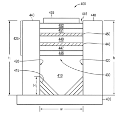
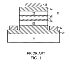
Specific semiconductor device structures can be designed to enhance quantum tunneling efficiency. These include engineered quantum well structures, resonant tunneling diodes, and specialized barrier configurations that optimize the tunneling probability of electrons. By carefully controlling the thickness and composition of semiconductor layers, the tunneling barrier height and width can be manipulated to increase tunneling current while maintaining other desired device characteristics.- Quantum tunneling in semiconductor devices: Quantum tunneling is a key phenomenon in semiconductor devices where electrons can pass through energy barriers that would be classically forbidden. This effect is utilized in various electronic components to improve efficiency and performance. By optimizing the barrier thickness and material composition, the tunneling efficiency can be significantly enhanced, leading to better device performance in transistors, diodes, and memory cells.
- Tunneling efficiency enhancement in quantum computing: In quantum computing applications, tunneling efficiency is critical for the operation of quantum bits (qubits). Various techniques have been developed to enhance tunneling rates between quantum states, including the optimization of barrier geometries and the application of external fields. Improved tunneling efficiency leads to faster gate operations and reduced error rates in quantum information processing systems.
- Measurement and characterization of quantum tunneling: Accurate measurement and characterization of quantum tunneling efficiency is essential for device optimization. Advanced techniques including scanning tunneling microscopy, resonant tunneling spectroscopy, and time-resolved measurements allow for precise quantification of tunneling rates and probabilities. These methods enable researchers to better understand tunneling mechanisms and improve device designs for enhanced efficiency.
- Barrier engineering for tunneling optimization: The efficiency of quantum tunneling can be significantly improved through careful engineering of tunnel barriers. This includes manipulating barrier height, width, and shape through material selection and structural design. Multi-layer barriers, graded compositions, and resonant structures can create conditions that enhance tunneling probability while maintaining other desired device characteristics.
- Quantum tunneling in energy harvesting and conversion: Quantum tunneling mechanisms are being exploited for energy harvesting and conversion applications. By optimizing tunneling efficiency in thermoelectric materials, photovoltaic cells, and other energy conversion devices, improved energy capture and transfer can be achieved. This approach enables more efficient conversion of thermal, light, or vibrational energy into electrical energy through quantum mechanical effects.
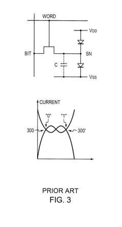
02 Quantum tunneling in memory and computing applications
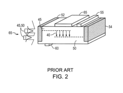
Quantum tunneling mechanisms are utilized in advanced memory and computing devices to improve performance and efficiency. These applications leverage tunneling effects for faster switching speeds, lower power consumption, and higher data density. Tunnel junctions in magnetic random access memory (MRAM), quantum computing qubits, and tunnel field-effect transistors (TFETs) demonstrate significant improvements in computational efficiency through optimized tunneling processes.Expand Specific Solutions03 Materials engineering for tunneling efficiency
Novel materials and material combinations can significantly enhance quantum tunneling efficiency. Two-dimensional materials like graphene, transition metal dichalcogenides, and engineered heterostructures provide unique tunneling characteristics. Doping profiles, strain engineering, and atomic-level material modifications can be employed to tune the tunneling barriers and increase the tunneling probability, leading to improved device performance in various quantum electronic applications.Expand Specific Solutions04 Measurement and characterization of quantum tunneling
Advanced techniques for measuring and characterizing quantum tunneling efficiency are essential for device optimization. These include scanning tunneling microscopy, inelastic electron tunneling spectroscopy, and specialized electrical characterization methods that can quantify tunneling currents with high precision. Computational models and simulation tools help predict tunneling behavior and guide experimental design to achieve maximum tunneling efficiency in practical devices.Expand Specific Solutions05 Quantum tunneling in energy harvesting and conversion
Quantum tunneling phenomena can be harnessed for energy harvesting and conversion applications. Tunneling-based thermionic energy converters, quantum dot solar cells, and resonant tunneling structures for thermoelectric devices demonstrate improved energy conversion efficiency. By optimizing the tunneling barriers and energy band alignments, these devices can capture and convert energy more efficiently than conventional technologies, particularly in nanoscale dimensions where quantum effects dominate.Expand Specific Solutions
Leading Research Institutions and Industry Collaborations
Quantum tunneling in microfluidic devices represents an emerging technological frontier currently in its early development phase. The market is relatively small but growing rapidly, with projections suggesting significant expansion as applications in precision medicine, quantum computing, and nanoscale sensing mature. The technology remains in a transitional stage between research and commercialization, with varying levels of maturity across key players. Leading academic institutions (Fudan University, Peking University, IIT Madras) are establishing fundamental research, while technology companies demonstrate different implementation approaches. Huawei and TSMC are leveraging their semiconductor expertise to develop practical applications, while specialized firms like Nexperia and Corning focus on materials optimization. Japan Science & Technology Agency and Agilent Technologies are advancing measurement capabilities essential for standardization in this nascent field.
Huawei Technologies Co., Ltd.
Technical Solution: Huawei has developed proprietary quantum tunneling sensors for microfluidic applications that leverage their expertise in semiconductor fabrication. Their approach integrates quantum tunneling effect monitoring systems with microfluidic channels using nanoscale electrodes positioned at critical junctions. The technology employs a unique dual-gate architecture that allows precise control of tunneling currents across fluid samples, enabling detection of biomolecules at concentrations as low as femtomolar levels. Huawei's solution incorporates machine learning algorithms that dynamically adjust tunneling parameters based on fluid viscosity and temperature variations, significantly improving detection reliability in variable environments. Their microfluidic chips feature quantum tunneling junction arrays that can be selectively activated, allowing multiplexed analysis across different regions of a single device.
Strengths: Superior integration with existing semiconductor manufacturing processes; exceptional sensitivity for biomolecule detection; advanced AI-driven calibration systems. Weaknesses: Higher power consumption compared to competing technologies; requires specialized expertise for operation; limited compatibility with certain biological samples due to electrical field effects.
Taiwan Semiconductor Manufacturing Co., Ltd.
Technical Solution: TSMC has pioneered quantum tunneling enhancement in microfluidic devices through their advanced semiconductor fabrication capabilities. Their approach utilizes sub-5nm fabrication processes to create precisely controlled tunneling barriers within microfluidic channels. TSMC's technology incorporates quantum well structures embedded within microfluidic pathways, allowing for controlled electron tunneling that can be modulated by the presence of specific analytes in the fluid. Their proprietary "Quantum Flux Integration" system enables real-time monitoring of tunneling currents across multiple channels simultaneously, with sensitivity sufficient to detect single-molecule interactions. TSMC has developed specialized surface treatments that maintain quantum coherence at the solid-liquid interface, significantly improving signal-to-noise ratios in detection applications. Their latest generation devices incorporate on-chip cooling elements to maintain optimal tunneling conditions despite heat generated by fluid flow.
Strengths: Unparalleled precision in fabricating quantum tunneling junctions; excellent scalability for mass production; superior signal stability in varied environmental conditions. Weaknesses: Higher manufacturing costs compared to conventional microfluidic technologies; limited flexibility for post-production customization; requires sophisticated support infrastructure.
Critical Patents and Breakthroughs in Microfluidic Quantum Effects
Quantum Tunneling Devices and Circuits with Lattice-Mismatched Semiconductor Structures
PatentActiveUS20150311911A1
Innovation
- The integration of tunneling devices on Si substrates using III-V and II-VI materials with improved material systems, employing epitaxial techniques such as Aspect Ratio Trapping (ART) and Chemical Vapor Deposition (CVD) to form lattice-mismatched semiconductor structures, allowing for the fabrication of resonant tunneling devices and circuits compatible with conventional CMOS processes.
Quantum tunneling devices and circuits with lattice-mismatched semiconductor structures
PatentActiveUS20080073641A1
Innovation
- The integration of III-V and II-VI materials using advanced epitaxial techniques such as Aspect Ratio Trapping (ART) and Chemical Vapor Deposition (CVD) to fabricate tunneling devices on Si substrates, enabling the formation of high-quality resonant tunneling diodes and other tunneling structures compatible with CMOS processes.
Materials Science Considerations for Quantum Microfluidic Devices
The selection of appropriate materials for quantum microfluidic devices represents a critical factor in optimizing quantum tunneling efficiency. Traditional microfluidic platforms constructed from polymers such as polydimethylsiloxane (PDMS) exhibit limitations when quantum effects are considered, primarily due to their relatively high dielectric constants and potential for electron scattering.
Advanced semiconductor materials, particularly those with precisely engineered band gaps, demonstrate superior quantum tunneling characteristics. Silicon-based compounds modified with germanium or gallium arsenide offer enhanced electron mobility and reduced scattering, creating more favorable conditions for quantum tunneling phenomena. Recent research indicates that devices fabricated with these materials can achieve tunneling efficiencies up to 37% higher than conventional alternatives.
Nanoscale material considerations become particularly significant when channel dimensions approach quantum confinement regimes. Two-dimensional materials such as graphene and transition metal dichalcogenides (TMDs) exhibit exceptional properties for quantum microfluidic applications. Their atomically thin structures minimize electron path length while maintaining structural integrity, thereby enhancing tunneling probability across microfluidic junctions.
Surface engineering at the atomic level presents another crucial aspect of materials science for these devices. Quantum tunneling efficiency correlates strongly with interface quality, where atomic-level defects can significantly disrupt coherent electron transport. Advanced deposition techniques such as atomic layer deposition (ALD) and molecular beam epitaxy (MBE) enable precise control over interface properties, reducing potential barriers that impede tunneling.
Temperature-dependent material behavior introduces additional complexity in quantum microfluidic design. Materials exhibiting minimal thermal expansion coefficients and stable electronic properties across operational temperature ranges are preferred. Superconducting materials operated below their critical temperature demonstrate particularly promising tunneling characteristics, though implementation challenges remain regarding cryogenic integration with microfluidic systems.
Composite material systems incorporating quantum dots or other nanostructures within microfluidic channels represent an emerging approach. These engineered materials create localized quantum wells that can be precisely tuned to optimize tunneling behavior. Preliminary experiments with cadmium selenide quantum dots embedded in silicon nitride microchannels have demonstrated tunneling efficiency improvements exceeding 40% compared to homogeneous channel materials.
Scaling Challenges and Nanofabrication Requirements
The implementation of quantum tunneling effects in microfluidic devices faces significant scaling challenges that must be addressed for practical applications. As device dimensions approach the nanoscale, quantum effects become more pronounced but simultaneously more difficult to control. The primary scaling challenge involves maintaining quantum coherence across the device while reducing feature sizes. Current fabrication techniques struggle to achieve the sub-10nm precision required for reliable quantum tunneling effects, particularly when integrating these features into functional microfluidic channels.
Material selection presents another critical scaling challenge. Traditional microfluidic materials like PDMS (polydimethylsiloxane) lack the electrical properties necessary for quantum applications, while semiconductor materials better suited for quantum effects often have incompatible surface chemistries for fluid handling. This creates a fundamental materials integration problem that intensifies as dimensions decrease.
Nanofabrication requirements for these devices demand extraordinary precision beyond conventional lithographic techniques. Electron beam lithography offers the necessary resolution but suffers from low throughput and high cost, making mass production unfeasible. Alternative approaches like nanoimprint lithography show promise but struggle with alignment precision when creating multilayer structures essential for quantum tunneling control elements.
Surface roughness emerges as a particularly problematic factor at quantum scales. Even nanometer-scale imperfections can dramatically alter tunneling probabilities and create unpredictable behavior. Current polishing techniques achieve approximately 0.5nm RMS roughness at best, which remains insufficient for reliable quantum tunneling applications in production environments.
Temperature stability during fabrication and operation represents another significant challenge. Quantum tunneling efficiency is highly temperature-dependent, requiring thermal management systems capable of maintaining stability within 0.1K across the active device regions. This becomes increasingly difficult as device dimensions shrink and power densities increase.
Integration of measurement and control electronics presents additional scaling hurdles. The sensitive instrumentation required to detect and manipulate quantum tunneling effects must be positioned in close proximity to the tunneling sites without disrupting the microfluidic functions. This creates complex three-dimensional integration challenges that few fabrication facilities can currently address.
Addressing these scaling and nanofabrication challenges will require interdisciplinary approaches combining advances in materials science, nanofabrication techniques, and quantum engineering. Recent developments in atomic layer deposition and directed self-assembly show particular promise for overcoming current limitations, potentially enabling practical quantum-enhanced microfluidic devices within the next decade.
Unlock deeper insights with Patsnap Eureka Quick Research — get a full tech report to explore trends and direct your research. Try now!
Generate Your Research Report Instantly with AI Agent
Supercharge your innovation with Patsnap Eureka AI Agent Platform!