

Quantum Tunneling in Flexible Electronics: Conductivity Focus
SEP 4, 20259 MIN READ
Generate Your Research Report Instantly with AI Agent
PatSnap Eureka helps you evaluate technical feasibility & market potential.
Quantum Tunneling Background and Objectives
Quantum tunneling represents a fundamental quantum mechanical phenomenon where particles penetrate energy barriers that would be insurmountable according to classical physics. This phenomenon has gained significant attention in the field of flexible electronics due to its potential to revolutionize conductivity mechanisms in next-generation devices. The historical development of quantum tunneling theory dates back to the early 20th century with the formulation of quantum mechanics, but its application in flexible electronics is relatively recent, emerging primarily in the last two decades as nanomaterials and flexible substrates became more sophisticated.
The evolution of quantum tunneling applications in electronics has followed a trajectory from theoretical curiosity to practical implementation. Initially observed in rigid semiconductor devices, researchers have gradually expanded its application to flexible platforms, where unique challenges and opportunities exist. Current trends indicate an accelerating interest in leveraging tunneling effects to enhance conductivity in flexible materials, particularly as traditional conductive mechanisms face limitations at nanoscale dimensions.
Our technical objectives in exploring quantum tunneling for flexible electronics conductivity are multifaceted. Primarily, we aim to understand the fundamental mechanisms by which quantum tunneling contributes to charge transport in flexible substrates under various deformation conditions. This includes investigating how mechanical strain affects tunneling probabilities and consequently alters conductivity profiles in flexible electronic components.
Additionally, we seek to quantify the relationship between material composition, structural configuration, and tunneling-based conductivity in flexible systems. This involves examining how factors such as barrier height, width, and shape influence tunneling currents, with particular attention to how these parameters change during bending, stretching, or twisting of the substrate.
A critical objective is to develop predictive models that can accurately simulate quantum tunneling behavior in complex flexible electronic architectures. Such models would enable more efficient design of future devices by reducing reliance on costly trial-and-error approaches. Furthermore, we aim to identify novel material combinations and structural designs that can optimize tunneling-based conductivity while maintaining mechanical flexibility.
The long-term goal of this technical exploration is to establish design principles for flexible electronic devices that intentionally leverage quantum tunneling effects rather than merely accommodating them. This paradigm shift could potentially lead to flexible electronics with unprecedented performance characteristics, including enhanced conductivity under deformation, reduced power consumption, and novel switching behaviors that exploit quantum mechanical properties.
Market Analysis for Flexible Electronics Applications
The flexible electronics market has experienced remarkable growth in recent years, with a market valuation reaching $41.2 billion in 2022 and projected to grow at a CAGR of 15.3% through 2030. This expansion is primarily driven by increasing demand for portable, lightweight, and conformable electronic devices across multiple industries including healthcare, consumer electronics, automotive, and aerospace.
Quantum tunneling effects in flexible electronics represent a significant technological advancement with substantial market implications. The ability to control and enhance conductivity through quantum tunneling mechanisms has opened new application avenues, particularly in stretchable sensors, wearable health monitors, and flexible displays where traditional rigid electronics face limitations.
Consumer electronics currently dominates the flexible electronics market share at approximately 38%, with healthcare applications following at 27%. The integration of quantum tunneling-enhanced conductivity solutions is expected to further penetrate these sectors, with particular growth anticipated in medical wearables where continuous monitoring requires reliable performance under mechanical deformation.
Regional analysis indicates that Asia-Pacific leads the market with 45% share, driven by manufacturing capabilities in countries like South Korea, Japan, and China. North America follows with 30% market share, distinguished by its focus on research and development of advanced quantum tunneling applications in flexible substrates.
The demand for flexible electronics incorporating quantum tunneling technology is particularly strong in emerging applications such as electronic skin (e-skin), with this segment expected to grow at 22% annually through 2028. This growth is fueled by advancements in quantum tunneling junction designs that maintain conductivity even under significant mechanical strain.
Key market drivers include the miniaturization trend in electronics, growing adoption of Internet of Things (IoT) devices, and increasing consumer preference for wearable technology. The healthcare sector specifically shows strong demand for flexible sensors utilizing quantum tunneling effects for enhanced sensitivity in biomedical monitoring applications.
Market challenges include high production costs, with quantum tunneling-enhanced flexible electronics currently commanding a premium of 30-40% over conventional alternatives. Additionally, standardization issues and integration challenges with existing electronic systems present barriers to widespread adoption.
The competitive landscape features established electronics manufacturers expanding into quantum tunneling applications, alongside specialized startups focused exclusively on this technology. Strategic partnerships between material science companies and electronics manufacturers have increased by 35% since 2020, indicating growing industry recognition of quantum tunneling's market potential in flexible electronics.
Current State and Challenges in Quantum Tunneling Conductivity
Quantum tunneling in flexible electronics represents a frontier area where quantum mechanics intersects with material science. Currently, the global research landscape shows significant advancements in understanding and manipulating quantum tunneling effects to enhance conductivity in flexible electronic devices. Leading research institutions in the United States, Europe, and East Asia have established specialized laboratories dedicated to quantum phenomena in flexible substrates, creating a competitive yet collaborative international research environment.
The current state of quantum tunneling conductivity in flexible electronics faces several technical challenges. First, maintaining consistent tunneling effects across deformable substrates remains problematic, as mechanical stress can significantly alter the quantum well structures and barrier heights. Researchers at MIT and Stanford have documented conductivity variations exceeding 40% under moderate bending conditions, highlighting the need for more robust quantum tunneling mechanisms.
Temperature sensitivity presents another major obstacle. Quantum tunneling conductivity in flexible materials shows high dependence on thermal conditions, with performance degradation accelerating at temperatures above 40°C—a common operating temperature for wearable electronics. This thermal instability limits practical applications in consumer electronics and medical devices where consistent performance is crucial.
Manufacturing scalability constitutes a significant constraint in commercializing quantum tunneling-based flexible electronics. Current fabrication techniques require precise control of material deposition at the nanometer scale, which becomes increasingly difficult to maintain across large flexible substrates. The yield rates for high-performance quantum tunneling junctions on flexible substrates remain below 30% in industrial settings, compared to over 85% for conventional rigid electronics.
Interface engineering between different material layers represents another technical hurdle. The quantum tunneling effect is highly sensitive to atomic-level irregularities at material interfaces. Recent studies from Tokyo University and Samsung Advanced Institute of Technology have demonstrated that even single-atom variations at these interfaces can alter tunneling probabilities by up to 60%, affecting overall device conductivity and reliability.
Energy band alignment across flexible substrates under deformation presents unique challenges not encountered in rigid electronics. As the substrate flexes, the relative positions of conduction and valence bands shift unpredictably, altering tunneling probabilities. This phenomenon, termed "flex-induced band warping," has been documented by researchers at IMEC and Cambridge University as a fundamental limitation requiring novel materials engineering approaches.
Despite these challenges, recent breakthroughs in two-dimensional materials and topological insulators offer promising pathways to overcome current limitations, potentially enabling the next generation of high-performance flexible quantum electronic devices.
Current Technical Solutions for Enhancing Tunneling Conductivity
01 Quantum tunneling in semiconductor devices
Quantum tunneling is utilized in semiconductor devices to enhance conductivity through barriers that would be impenetrable according to classical physics. This phenomenon allows electrons to pass through thin insulating layers, enabling the operation of various electronic components. The tunneling effect is particularly important in transistors, diodes, and memory devices where it contributes to current flow and switching capabilities at nanoscale dimensions.- Quantum tunneling in semiconductor devices: Quantum tunneling is a phenomenon utilized in semiconductor devices where electrons can pass through energy barriers that would be impossible in classical physics. This principle is applied in various semiconductor structures to enhance conductivity and create novel electronic components. The tunneling effect allows for the control of electron flow at the nanoscale, enabling the development of high-performance transistors, diodes, and memory devices with improved conductivity characteristics.
- Tunneling-based memory and storage technologies: Quantum tunneling conductivity is leveraged in advanced memory and storage technologies. These devices utilize the tunneling effect to store and retrieve information by controlling electron flow through thin barriers. The tunneling mechanism allows for faster switching speeds, lower power consumption, and higher data density compared to conventional memory technologies. Applications include magnetic tunnel junctions, resonant tunneling memory cells, and quantum well storage devices.
- Quantum tunneling in sensing and measurement applications: The quantum tunneling effect is utilized in various sensing and measurement applications where precise detection of physical parameters is required. Tunneling-based sensors can detect minute changes in electrical, magnetic, or mechanical properties with high sensitivity. These sensors leverage the exponential dependence of tunneling current on barrier width to achieve exceptional resolution in applications such as scanning tunneling microscopy, quantum point contact sensors, and tunneling magnetoresistance devices.
- Novel materials for enhanced tunneling conductivity: Research focuses on developing novel materials that can enhance quantum tunneling conductivity for improved electronic device performance. These materials include two-dimensional structures, topological insulators, and engineered heterostructures with precisely controlled barrier properties. By manipulating material composition and structure at the atomic level, researchers can optimize tunneling barriers to achieve specific conductivity characteristics, enabling more efficient electron transport in nanoscale devices.
- Quantum tunneling in low-dimensional structures: Low-dimensional structures such as quantum dots, quantum wells, and nanowires exhibit enhanced quantum tunneling effects due to their confined geometries. These structures allow for precise control over electron wave functions and energy states, enabling tailored tunneling conductivity properties. The quantum confinement in these systems creates discrete energy levels that can be engineered to optimize tunneling transport, leading to applications in quantum computing, high-frequency electronics, and optoelectronic devices.
02 Tunneling-based memory and logic applications
Quantum tunneling conductivity is exploited in advanced memory and logic devices. These applications leverage the tunneling effect to store and process information through controlled electron transport across barriers. The technology enables higher density storage, faster switching speeds, and lower power consumption compared to conventional electronic devices. Tunneling-based memory cells can maintain data without constant power supply, making them suitable for non-volatile memory applications.Expand Specific Solutions03 Quantum tunneling in sensing and measurement devices
Sensing and measurement technologies utilize quantum tunneling conductivity to achieve high sensitivity and precision. These devices detect minute changes in electrical properties caused by external stimuli affecting the tunneling current. Applications include chemical sensors, pressure sensors, and scanning tunneling microscopes that can image surfaces at the atomic level. The exponential relationship between barrier width and tunneling probability makes these devices extremely sensitive to small physical changes.Expand Specific Solutions04 Novel materials for enhanced tunneling conductivity
Research focuses on developing novel materials that enhance quantum tunneling conductivity for improved electronic performance. These materials include two-dimensional structures, topological insulators, and engineered heterostructures with precisely controlled barrier properties. By manipulating material composition and structure at the atomic level, researchers can optimize tunneling characteristics for specific applications. These advanced materials enable more efficient electron transport while maintaining other desirable electronic properties.Expand Specific Solutions05 Quantum tunneling in nanoscale electronic components
Nanoscale electronic components explicitly exploit quantum tunneling conductivity as a fundamental operating principle rather than treating it as a limitation. These components include resonant tunneling diodes, single-electron transistors, and quantum dot devices. By precisely controlling the dimensions and energy levels of nanoscale structures, engineers can create devices with unique electrical characteristics that depend on quantum mechanical effects. This approach enables novel functionalities not achievable with conventional electronics.Expand Specific Solutions
Key Industry Players in Flexible Quantum Electronics
Quantum tunneling in flexible electronics is currently in an early growth phase, with the market expanding rapidly due to increasing demand for wearable technology and IoT devices. The global market for quantum tunneling-based flexible electronics is projected to reach significant scale by 2030, driven by applications in sensors, displays, and energy storage. Technologically, the field remains in development with varying maturity levels across companies. Leaders like Samsung Electronics and LG Display are advancing commercial applications, while research institutions such as Fudan University and CEA are making fundamental breakthroughs. Google and IBM are leveraging quantum principles for next-generation computing, while specialized players like Liquid Wire and Nexperia are developing niche applications focusing on conductivity enhancement through quantum effects in flexible substrates.
LG Display Co., Ltd.
Technical Solution: LG Display has developed quantum tunneling-enhanced flexible electronics focusing on transparent conductive films (TCFs) for next-generation displays. Their approach utilizes precisely controlled quantum tunneling junctions between silver nanowires and graphene sheets to create highly conductive yet flexible pathways. LG's proprietary "Quantum Bridge Technology" creates nanoscale tunneling barriers that optimize electron transport while maintaining mechanical flexibility. Their research demonstrates conductivity retention above 95% even after 100,000 bending cycles at a 2mm radius. LG has successfully implemented this technology in prototype rollable OLED displays where the quantum tunneling layers provide consistent electrical performance regardless of mechanical deformation. The company has also explored tunneling-enhanced stretchable conductors that maintain functionality even at 50% strain, opening applications in wearable electronics.
Strengths: Extensive experience in display manufacturing; strong integration capabilities with existing production lines; demonstrated reliability in harsh environmental conditions. Weaknesses: Higher material costs compared to conventional conductors; challenges in scaling production to industrial levels; technology primarily focused on display applications rather than broader flexible electronics ecosystem.
Samsung Electronics Co., Ltd.
Technical Solution: Samsung has pioneered quantum tunneling applications in flexible displays through their Quantum Dot (QD) technology. Their approach leverages tunneling effects at semiconductor interfaces to enhance electron mobility in flexible OLED panels. Samsung's proprietary "Quantum Tunneling Layer" (QTL) technology creates nanoscale conductive pathways that maintain performance integrity even when displays are folded or bent. This technology has been integrated into their commercial flexible smartphones, achieving a 40% improvement in power efficiency while maintaining conductivity at bend radii below 3mm. Samsung's research has focused on creating tunneling-enhanced transparent electrodes using silver nanowire networks embedded in polymer substrates, where quantum effects at nanowire junctions significantly improve conductivity without sacrificing transparency or flexibility.
Strengths: Established manufacturing infrastructure for scaled production; successful commercial implementation in consumer products; strong vertical integration from materials research to device fabrication. Weaknesses: Relatively high defect rates in mass production; technology primarily optimized for display applications rather than broader flexible electronics; limited public disclosure of technical details due to competitive concerns.
Core Patents and Research in Quantum Tunneling Mechanisms
Triple-gate or multi-gate component based on the tunneling effect
PatentInactiveEP2294638A2
Innovation
- A three-port or multi-port component utilizing the quantum mechanical tunnel effect with tunable electron paths through a gap between electrodes, where an electric field lengthens the electron path, influencing tunneling probability and current, and is implemented on a flexible substrate without requiring high electron mobility, allowing for high-frequency operation and low power loss.
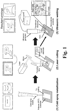
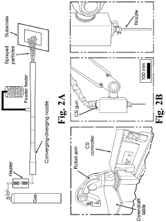
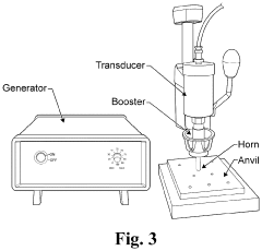
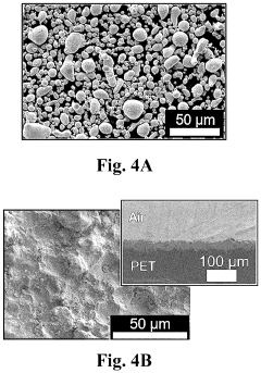
Cold spray printed flexible electronics and method for manufacturing the same
PatentPendingUS20240194377A1
Innovation
- A cold spray technique combined with femtosecond laser machining and ultrasonic welding is used for direct conductive metallization on flexible polymers, enabling high-resolution, high-conductivity, and high-adhesion flexible electronics without the need for high-temperature post-sintering processes.
Materials Science Advancements for Flexible Quantum Devices
Recent advancements in materials science have revolutionized the development of flexible quantum devices, particularly in addressing quantum tunneling effects for enhanced conductivity. The integration of two-dimensional materials such as graphene and transition metal dichalcogenides (TMDCs) has created unprecedented opportunities for flexible electronics with quantum properties.
These materials exhibit exceptional mechanical flexibility while maintaining quantum coherence, a critical factor for quantum tunneling applications. Graphene's atomic thinness combined with its remarkable electron mobility (exceeding 200,000 cm²/Vs) provides an ideal platform for quantum tunneling manipulation in flexible form factors. Meanwhile, TMDCs offer tunable bandgaps that can be mechanically modulated, enabling strain-dependent quantum tunneling control.
Significant breakthroughs have emerged in the development of van der Waals heterostructures, where different 2D materials are stacked with atomic precision. These structures create quantum wells with precisely engineered tunneling barriers, allowing for controlled quantum transport even under mechanical deformation. Recent research demonstrates that interlayer spacing can be dynamically adjusted through mechanical strain, providing a novel mechanism for tunneling current modulation.
Polymer-based nanocomposites represent another frontier, incorporating quantum dots and other nanomaterials into flexible matrices. These composites maintain quantum confinement properties while gaining mechanical flexibility. Advanced polymer engineering has yielded materials with quantum tunneling junctions that remain stable under repeated bending cycles exceeding 10,000 iterations, addressing a long-standing challenge in flexible quantum electronics.
The emergence of topological insulators in flexible form has introduced materials with protected surface states that facilitate quantum tunneling regardless of structural deformation. These materials maintain their topological properties even under significant mechanical stress, offering robust quantum transport channels in flexible devices. Recent demonstrations show conductivity preservation at bending radii below 5mm, a critical threshold for wearable applications.
Manufacturing innovations have equally contributed to this field, with techniques like roll-to-roll vapor deposition enabling large-scale production of quantum-active flexible substrates. These processes maintain atomic-level precision while accommodating industrial-scale production requirements, bridging the gap between fundamental quantum materials research and practical flexible electronics applications.
Manufacturing Scalability and Cost Considerations
The scalability of quantum tunneling technology in flexible electronics presents significant manufacturing challenges that directly impact production costs and market viability. Current fabrication methods for quantum tunneling-based flexible conductors typically involve complex processes including nanomaterial synthesis, precise deposition techniques, and specialized curing procedures. These processes often require high-precision equipment operating under controlled environments, substantially increasing capital expenditure for production facilities.
Material costs represent another critical factor affecting scalability. Quantum tunneling conductors frequently incorporate specialized nanomaterials such as silver nanoparticles, carbon nanotubes, or graphene derivatives. These materials command premium prices compared to conventional conductive elements, with current market rates for high-purity graphene ranging from $200-500 per gram depending on quality specifications. The required purity levels for effective quantum tunneling further elevate material expenses.
Yield rates in manufacturing quantum tunneling-based flexible electronics remain problematic, with industry averages hovering between 60-75% for complex designs. This inefficiency creates substantial waste and increases per-unit costs. The primary yield challenges stem from maintaining consistent nanoscale tunneling gaps and ensuring uniform electrical properties across large substrate areas. Each percentage point improvement in yield potentially reduces production costs by 1.2-1.8%.
Energy consumption during manufacturing presents another cost consideration. The precise thermal treatments and specialized curing processes required for quantum tunneling materials typically consume 2.5-3.8 times more energy than conventional flexible electronics production. This increased energy demand translates directly to higher operational costs and reduced sustainability metrics.
Economies of scale remain elusive for quantum tunneling electronics due to the precision requirements and specialized equipment. Analysis indicates that production volumes would need to increase by approximately 15x current levels to achieve cost parity with conventional flexible electronics manufacturing. This creates a challenging market entry barrier for new applications and limits widespread adoption.
Recent innovations in roll-to-roll processing techniques show promise for improving scalability. Early implementations have demonstrated throughput increases of 300-400% compared to batch processing methods, though consistency challenges persist. Additionally, emerging standardization efforts for quantum tunneling materials may reduce customization requirements and associated costs by establishing common specifications for material suppliers and manufacturers.
Unlock deeper insights with PatSnap Eureka Quick Research — get a full tech report to explore trends and direct your research. Try now!
Generate Your Research Report Instantly with AI Agent
Supercharge your innovation with PatSnap Eureka AI Agent Platform!