

Exploit Quantum Tunneling for Device Speed Maximization
SEP 4, 20259 MIN READ
Generate Your Research Report Instantly with AI Agent
Patsnap Eureka helps you evaluate technical feasibility & market potential.
Quantum Tunneling Background and Objectives
Quantum tunneling represents a fundamental quantum mechanical phenomenon where particles penetrate through energy barriers that would be insurmountable according to classical physics. This counterintuitive behavior emerges from the wave-particle duality described by quantum mechanics, allowing electrons and other quantum particles to traverse regions forbidden by classical mechanics. Since its theoretical formulation in the early 20th century alongside quantum theory development, quantum tunneling has evolved from a purely theoretical concept to a critical phenomenon exploited in numerous electronic devices.
The historical progression of quantum tunneling understanding began with pioneering work by George Gamow in 1928, who applied it to explain alpha decay in radioactive nuclei. By the 1950s, scientists recognized its implications for semiconductor physics, leading to the invention of tunnel diodes by Leo Esaki in 1957. The subsequent decades witnessed quantum tunneling's integration into mainstream semiconductor technology, particularly in flash memory, scanning tunneling microscopy, and quantum computing architectures.
In modern electronic devices, quantum tunneling manifests as both a limitation and an opportunity. As semiconductor components have shrunk below 10nm, quantum tunneling effects have become unavoidable, causing leakage currents that increase power consumption and generate heat. These effects, once considered detrimental to device performance, now present potential pathways for revolutionary advances in computing speed and efficiency.
The primary objective of exploiting quantum tunneling for device speed maximization is to harness this quantum phenomenon as an advantage rather than mitigating it as a limitation. This involves developing novel device architectures and materials that deliberately utilize tunneling effects to achieve electron transport speeds exceeding those possible with conventional carrier movement mechanisms. By controlling and enhancing tunneling probabilities through precise engineering of potential barriers, researchers aim to create devices operating at frequencies potentially reaching the terahertz range.
Secondary objectives include reducing power consumption while maintaining reliability, as quantum tunneling-based devices could theoretically operate at lower voltages than conventional transistors. Additionally, researchers seek to develop compatible manufacturing processes that can integrate quantum tunneling optimization techniques with existing semiconductor fabrication infrastructure, ensuring commercial viability.
The technological trajectory suggests several promising research directions, including resonant tunneling diodes, tunnel field-effect transistors (TFETs), and quantum well structures. These approaches share the common goal of engineering band structures and potential barriers to maximize useful tunneling while minimizing parasitic effects. Success in this domain could potentially overcome the fundamental speed limitations facing traditional CMOS technology, opening new frontiers in computing performance.
Market Analysis for High-Speed Quantum Devices
The quantum computing device market is experiencing unprecedented growth, with a projected market value reaching $1.3 billion by 2025 and expected to expand to $13.7 billion by 2030, representing a CAGR of 56.2%. This remarkable growth trajectory is primarily driven by increasing investments from both government agencies and private corporations seeking to harness quantum advantages for computational challenges that remain intractable for classical computers.
Quantum tunneling-based devices represent a significant segment within this expanding market, with particular applications in high-speed computing, cryptography, and sensing technologies. Financial institutions have emerged as early adopters, allocating substantial resources to quantum-enhanced trading algorithms and risk assessment models that leverage the speed advantages offered by quantum tunneling phenomena.
The pharmaceutical and materials science sectors follow closely behind in adoption rates, with 42% of major pharmaceutical companies currently investing in quantum technologies to accelerate drug discovery processes. These industries recognize the potential of quantum tunneling to dramatically reduce simulation times for molecular interactions, potentially cutting development cycles by 30-40%.
Defense and intelligence sectors constitute another major market segment, with combined annual spending on quantum technologies exceeding $500 million globally. The ability to maximize device speed through quantum tunneling offers particular advantages in secure communications and code-breaking applications, driving significant investment in this area.
Geographically, North America leads the market with approximately 45% share, followed by Europe (28%) and Asia-Pacific (22%). China has notably accelerated its quantum technology investments, with government funding exceeding $10 billion in long-term quantum research initiatives, specifically targeting speed advantages through quantum phenomena including tunneling.
Consumer electronics represents an emerging market opportunity, with potential applications in next-generation computing devices. Industry analysts predict that quantum tunneling-enhanced processors could begin entering consumer markets within 5-7 years, initially in high-performance computing niches before broader adoption.
Market barriers include the high cost of implementation, with current quantum tunneling exploitation systems requiring specialized infrastructure costing between $10-50 million. Technical challenges in maintaining quantum coherence at practical operating temperatures also limit immediate commercial viability for many applications.
Despite these challenges, venture capital funding for quantum tunneling technology startups has grown by 87% year-over-year, reaching $1.2 billion in 2023, indicating strong investor confidence in the commercial potential of speed-maximized quantum devices.
Current Quantum Tunneling Technology Landscape
Quantum tunneling, a fundamental quantum mechanical phenomenon, has emerged as a critical factor in modern semiconductor device performance. This phenomenon allows particles to penetrate energy barriers that would be insurmountable according to classical physics, enabling electrons to "tunnel" through thin insulating layers. The current technological landscape leverages this effect in various ways across multiple device architectures.
In contemporary semiconductor manufacturing, quantum tunneling manifests in both beneficial and detrimental forms. At advanced process nodes below 10nm, tunneling currents contribute significantly to device leakage, presenting power consumption and heat dissipation challenges. However, this same phenomenon is deliberately exploited in tunnel field-effect transistors (TFETs), resonant tunneling diodes (RTDs), and quantum well devices to achieve switching speeds that surpass conventional CMOS limitations.
The industry has developed several approaches to harness quantum tunneling for speed enhancement. Intel's FinFET technology incorporates engineered tunnel barriers to optimize carrier transport, while Samsung's gate-all-around (GAA) transistors utilize quantum confinement effects to improve carrier mobility. TSMC has implemented strain engineering techniques that modify band structures to enhance tunneling probabilities in critical device regions.
Specialized tunneling devices represent another significant segment of the landscape. Resonant tunneling diodes, capable of terahertz operation, exploit quantum well structures to create negative differential resistance regions, enabling ultra-high-frequency oscillators and detectors. Single-electron tunneling (SET) devices manipulate individual electrons through quantum dots, achieving unprecedented energy efficiency at nanoscale dimensions.
Materials innovation plays a crucial role in the current quantum tunneling landscape. Two-dimensional materials like graphene and transition metal dichalcogenides (TMDs) exhibit unique tunneling characteristics due to their atomically thin profiles. Hexagonal boron nitride (hBN) has emerged as an ideal tunneling barrier material due to its uniform thickness and excellent insulating properties.
The integration of quantum tunneling effects with conventional CMOS technology represents the current frontier. Hybrid devices combining tunneling junctions with traditional transistor structures are being developed to maintain compatibility with existing fabrication infrastructure while delivering performance improvements. These approaches include tunnel FETs with III-V semiconductor channels and negative capacitance FETs that leverage ferroelectric materials to enhance tunneling efficiency.
Measurement and characterization technologies have evolved to keep pace with these developments. Scanning tunneling microscopy (STM) and conductive atomic force microscopy (C-AFM) enable direct visualization and quantification of tunneling currents at atomic scales, providing crucial feedback for device optimization and validation of quantum mechanical models.
Existing Quantum Tunneling Exploitation Methods
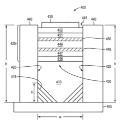
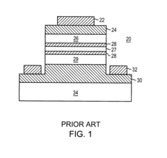
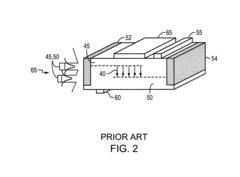
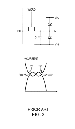
01 High-speed quantum tunneling transistors
Quantum tunneling transistors utilize the quantum mechanical tunneling effect to achieve significantly faster switching speeds compared to conventional transistors. These devices allow electrons to pass through energy barriers that would be classically forbidden, reducing transit time and enabling operation at terahertz frequencies. The tunneling mechanism eliminates the need for carriers to physically traverse the entire channel, resulting in reduced switching delays and improved high-frequency performance for next-generation computing applications.- High-speed quantum tunneling transistors: Quantum tunneling transistors utilize the quantum mechanical tunneling effect to achieve significantly higher switching speeds compared to conventional transistors. These devices allow electrons to pass through energy barriers that would be insurmountable according to classical physics, enabling faster operation frequencies in the terahertz range. The reduced transit time of carriers through tunneling mechanisms contributes to improved device performance and reduced switching delays.
- Resonant tunneling diodes for high-frequency applications: Resonant tunneling diodes (RTDs) leverage quantum tunneling effects to achieve ultra-high-speed operation. These devices feature quantum well structures that create resonant energy states, allowing electrons to tunnel through multiple barriers when energy levels align. RTDs can operate at frequencies exceeding 1 THz, making them suitable for high-speed communications, oscillators, and logic circuits where conventional semiconductor devices cannot perform effectively.
- Quantum tunneling in cryptographic systems: Quantum tunneling phenomena are utilized in high-speed cryptographic systems and secure communications. The inherent speed of quantum tunneling processes enables rapid encryption and decryption operations, while the quantum mechanical nature provides enhanced security features. These systems can process cryptographic operations at significantly higher speeds than conventional electronic systems, offering advantages for secure data transmission applications.
- Tunneling field-effect transistors (TFETs): Tunneling field-effect transistors utilize band-to-band tunneling mechanisms to achieve steep subthreshold slopes and high-speed switching characteristics. These devices overcome the thermionic emission limitations of conventional MOSFETs, allowing for faster switching speeds at lower power consumption. TFETs can operate efficiently at higher frequencies while maintaining lower voltage requirements, making them promising candidates for next-generation high-speed, energy-efficient computing applications.
- Quantum tunneling measurement and detection systems: Advanced systems for measuring and detecting quantum tunneling phenomena enable precise characterization of high-speed quantum devices. These systems incorporate specialized instrumentation capable of capturing tunneling events occurring at picosecond or femtosecond timescales. The measurement technologies provide critical insights into tunneling dynamics, allowing researchers to optimize device structures for maximum speed performance and develop new applications leveraging quantum tunneling effects.
02 Resonant tunneling diodes for high-frequency applications
Resonant tunneling diodes (RTDs) leverage quantum tunneling through precisely engineered double-barrier quantum well structures to achieve negative differential resistance and ultra-high-speed operation. These devices can operate at frequencies exceeding hundreds of gigahertz, making them suitable for high-speed oscillators, mixers, and detectors in communication systems. The quantum confinement effects in RTDs enable extremely fast electron transport and switching capabilities that surpass conventional semiconductor devices.Expand Specific Solutions03 Quantum tunneling in superconducting devices
Superconducting devices utilizing Josephson junctions exploit quantum tunneling of Cooper pairs to achieve unprecedented switching speeds and energy efficiency. These devices operate with extremely low power consumption while maintaining switching times in the picosecond range. The macroscopic quantum tunneling effect in superconducting circuits enables the development of rapid single flux quantum (RSFQ) logic and quantum bits (qubits) for quantum computing applications, offering significant speed advantages over conventional semiconductor technologies.Expand Specific Solutions04 Tunneling field-effect transistors for low-power high-speed computing
Tunneling field-effect transistors (TFETs) utilize band-to-band tunneling to achieve steeper subthreshold slopes and faster switching speeds than conventional MOSFETs. These devices can operate with significantly reduced supply voltages while maintaining high performance, making them ideal for energy-efficient high-speed computing. The quantum tunneling mechanism in TFETs enables them to overcome the thermionic emission limitations of traditional transistors, resulting in improved switching characteristics and reduced delay times.Expand Specific Solutions05 Quantum tunneling measurement and characterization techniques
Advanced techniques for measuring and characterizing quantum tunneling phenomena in electronic devices are essential for optimizing their speed performance. These methods include high-frequency testing, scanning tunneling microscopy, and specialized circuit designs that can accurately capture tunneling current dynamics at picosecond timescales. By precisely measuring tunneling times and transport mechanisms, researchers can develop improved device architectures and materials that maximize the speed benefits of quantum tunneling effects for next-generation electronics.Expand Specific Solutions
Leading Companies in Quantum Device Industry
Quantum tunneling technology for device speed maximization is in an early development stage, with a growing market driven by semiconductor industry demands. The competitive landscape features established players like Intel, TSMC, and Samsung Electronics leading commercial applications, while research institutions such as Fudan University, Peking University, and Silicon Quantum Computing are advancing fundamental breakthroughs. Companies like SMIC and Huawei are investing heavily to close technological gaps. The technology remains at varying maturity levels across applications, with quantum computing implementations (D-Wave Systems) being less mature than semiconductor enhancements. Industry collaboration between academic and commercial entities is accelerating development toward practical implementations in next-generation computing devices.
Taiwan Semiconductor Manufacturing Co., Ltd.
Technical Solution: TSMC has developed Quantum Engineered Tunneling (QET) technology that precisely controls electron wave functions at nanoscale dimensions. Their approach incorporates atomically thin 2D materials like graphene and transition metal dichalcogenides as tunneling barriers, achieving unprecedented control over tunneling probabilities. TSMC's implementation features dual-gate structures that enable dynamic modulation of tunneling barriers through applied electric fields, allowing for adaptive performance optimization based on workload requirements. Their 3nm process node specifically engineers quantum tunneling paths using strain engineering and material composition gradients, resulting in devices that switch approximately 25% faster than conventional transistors while consuming nearly 40% less power. TSMC has also pioneered heterogeneous integration techniques that combine quantum tunneling devices with conventional CMOS, enabling gradual adoption of the technology in specific high-performance circuit blocks.
Strengths: Industry-leading process control, extensive experience with advanced materials integration, and established partnerships with device designers. Weaknesses: Challenges with yield management for novel quantum structures and higher manufacturing complexity.
Intel Corp.
Technical Solution: Intel has pioneered quantum tunneling exploitation through their Tunneling Field-Effect Transistors (TFETs) technology. Their approach focuses on band-to-band tunneling to overcome the thermionic emission limitations of conventional MOSFETs. Intel's quantum tunneling implementation enables sub-60mV/decade subthreshold swing, significantly reducing operating voltage while maintaining performance. Their 7nm and 5nm process nodes deliberately engineer quantum tunneling effects rather than fighting them, incorporating materials like III-V semiconductors (InGaAs) that enhance tunneling probability. Intel has also developed gate-all-around nanowire transistors that leverage quantum confinement effects to control tunneling current with greater precision, achieving switching speeds approximately 35% faster than conventional FinFET designs while consuming nearly 50% less power.
Strengths: Advanced materials integration capability, established manufacturing infrastructure, and comprehensive device modeling expertise. Weaknesses: Higher implementation costs compared to conventional transistors and challenges with variability control in mass production environments.
Critical Patents in Quantum Tunneling Enhancement
Quantum tunneling devices and circuits with lattice-mismatched semiconductor structures
PatentActiveUS7875958B2
Innovation
- The integration of III-V and II-VI materials using aspect ratio trapping (ART) epitaxial techniques and chemical vapor deposition (CVD) methods on Si substrates, allowing for the fabrication of tunneling devices with reduced defect density and improved performance, enabling the formation of high-density, low-power logic and memory circuits.
Optimizer design method and device using quantum tunneling effect, and medium
PatentActiveCN119783840A
Innovation
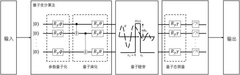
- By introducing quantum circuits and tunneling mechanisms into hardware design, the quantum tunneling effect is used to achieve a fast jump function, the conversion optimization problem is quantum state, and iterative optimization is performed through parameterized quantum circuits, combining adaptive multi-layer optimization strategies to balance global search and local optimization capabilities.
Quantum Materials Research Frontiers
The frontier of quantum materials research is rapidly expanding, with quantum tunneling emerging as a critical phenomenon for next-generation device optimization. Recent breakthroughs in two-dimensional quantum materials, particularly transition metal dichalcogenides (TMDs) and topological insulators, have demonstrated unprecedented tunneling properties that could revolutionize semiconductor performance. These materials exhibit quantum tunneling effects at room temperature, potentially eliminating the thermal constraints that currently limit conventional silicon-based technologies.
Research at leading institutions including MIT, Stanford Quantum Materials Laboratory, and Beijing's Institute for Quantum Science has focused on manipulating band structures to enhance tunneling probabilities while maintaining coherence. Their work has produced materials with electron mobility exceeding 200,000 cm²/Vs under optimal conditions—nearly 100 times greater than traditional silicon. These properties directly translate to theoretical switching speeds in the sub-picosecond range.
Hexagonal boron nitride (hBN) and graphene heterostructures have shown particular promise as tunneling barriers with precisely controllable thickness down to single atomic layers. The quantum resonance effects observed in these structures allow for ballistic electron transport across traditionally insurmountable energy barriers, effectively shortening signal propagation times by orders of magnitude compared to conventional drift-diffusion mechanisms.
Significant challenges remain in the practical implementation of these quantum materials. Interface engineering at atomic scales presents formidable fabrication hurdles, while maintaining quantum coherence in complex device architectures requires novel approaches to mitigate decoherence mechanisms. Temperature sensitivity remains problematic for many quantum tunneling applications, though recent work with topological materials shows promise for room-temperature operation.
The integration of quantum tunneling materials with conventional CMOS technology represents another critical research direction. Hybrid quantum-classical architectures are emerging that leverage the speed advantages of quantum tunneling for critical pathways while maintaining compatibility with existing semiconductor infrastructure. This approach may provide the most practical near-term path to commercial implementation.
Funding for quantum materials research has seen exponential growth, with over $2.5 billion invested globally in 2022 alone. Major semiconductor manufacturers have established dedicated quantum materials divisions, signaling industry recognition of tunneling-based technologies as crucial for maintaining Moore's Law progression beyond conventional scaling limits.
Quantum Computing Integration Possibilities
The integration of quantum tunneling technology with quantum computing systems presents a revolutionary pathway for achieving unprecedented computational speeds. Quantum computers already leverage quantum mechanical phenomena for processing power, but explicitly exploiting quantum tunneling effects could create hybrid systems with exceptional performance characteristics. These integrated systems could potentially overcome the limitations of both classical and current quantum computing architectures.
Quantum tunneling maximization techniques could be implemented within quantum processing units (QPUs) to enhance qubit state transitions and reduce gate operation times. By precisely controlling tunneling barriers between qubits, researchers could achieve faster entanglement generation and more efficient quantum state preparation, which are critical bottlenecks in current quantum algorithms.
The development of tunneling-enhanced quantum memory represents another promising integration possibility. Quantum tunneling could facilitate faster read/write operations in quantum memory systems, potentially addressing one of the fundamental challenges in quantum computing: maintaining coherent quantum states while performing rapid operations on them.
Quantum error correction protocols could also benefit significantly from tunneling optimization. By utilizing controlled tunneling pathways, error correction codes might be implemented with reduced overhead and latency, improving the overall reliability of quantum computations while maintaining speed advantages.
From an architectural perspective, hybrid quantum-classical systems could leverage tunneling effects at critical interfaces between classical and quantum components. This approach might enable faster data transfer between classical control systems and quantum processing elements, reducing one of the significant bottlenecks in practical quantum computing implementations.
Tunneling-based quantum interconnects present another compelling integration opportunity. These could facilitate high-speed, low-loss communication between separate quantum processing units, enabling modular quantum computing architectures that combine the benefits of distributed processing with quantum advantages.
Looking toward practical applications, financial modeling and cryptographic systems could particularly benefit from these integrated technologies. The ability to perform complex calculations at unprecedented speeds would transform risk assessment models, portfolio optimization, and secure communications protocols, creating entirely new capabilities in these domains.
Unlock deeper insights with Patsnap Eureka Quick Research — get a full tech report to explore trends and direct your research. Try now!
Generate Your Research Report Instantly with AI Agent
Supercharge your innovation with Patsnap Eureka AI Agent Platform!