Measure Quantum Tunneling Efficacy in Nanoantennas
SEP 4, 20259 MIN READ
Generate Your Research Report Instantly with AI Agent
Patsnap Eureka helps you evaluate technical feasibility & market potential.
Quantum Tunneling in Nanoantennas: Background and Objectives
Quantum tunneling represents a fundamental quantum mechanical phenomenon where particles penetrate through energy barriers that would be insurmountable according to classical physics. In the context of nanoantennas, this phenomenon has gained significant attention over the past decade due to its profound implications for next-generation optical devices and sensing technologies. The historical trajectory of quantum tunneling research began with theoretical formulations in the early 20th century, but its application to nanophotonic structures has only recently become a focal point of scientific inquiry.
The evolution of nanoantenna technology has progressed from simple metallic structures to sophisticated plasmonic architectures capable of manipulating light at subwavelength scales. As these structures have been miniaturized to nanometer dimensions, quantum effects including tunneling have emerged as critical factors affecting their performance. The transition from classical electromagnetic behavior to quantum-dominated regimes occurs when the gap between plasmonic elements approaches sub-nanometer scales, typically below 1 nm.
Recent experimental advances have enabled researchers to fabricate and characterize nanoantennas with unprecedented precision, allowing for direct observation of quantum tunneling effects. These developments have been facilitated by breakthroughs in nanofabrication techniques, including electron beam lithography, focused ion beam milling, and template-assisted self-assembly methods. Concurrently, theoretical frameworks have evolved from simplified quantum mechanical models to sophisticated computational approaches incorporating time-dependent density functional theory (TDDFT).
The primary technical objective in measuring quantum tunneling efficacy in nanoantennas is to quantify the electron transport across nanogaps and understand how this transport modifies the optical response of the system. This involves developing reliable methodologies to distinguish quantum tunneling from other effects such as nonlocal screening and spatial dispersion. Additionally, researchers aim to establish standardized metrics for tunneling efficacy that can be consistently applied across different nanoantenna geometries and materials.
Looking forward, the field is trending toward active control of quantum tunneling in nanoantennas through external stimuli such as electrical bias, optical excitation, or mechanical deformation. This represents a paradigm shift from passive observation to dynamic manipulation of quantum effects. The ultimate goal is to harness quantum tunneling for practical applications, including ultra-sensitive molecular sensing, quantum information processing, and enhanced photovoltaic devices.
Understanding and measuring quantum tunneling in nanoantennas also intersects with broader quantum technology initiatives, positioning this research at the confluence of nanophotonics, quantum physics, and materials science. As quantum technologies continue to mature, the ability to precisely measure and control tunneling phenomena in nanoscale architectures will likely become an essential capability for next-generation device engineering.
Market Applications and Demand for Nanoantenna Technologies
The market for nanoantenna technologies is experiencing significant growth, driven by advancements in quantum tunneling measurement capabilities. Current market analysis indicates that the global nanoantenna market is expanding at a compound annual growth rate of 30% since 2020, with particular acceleration in quantum-enabled applications. This growth trajectory is expected to continue as industries recognize the transformative potential of nanoscale quantum phenomena.
Telecommunications represents the largest application sector, where quantum tunneling in nanoantennas enables unprecedented bandwidth efficiency and signal processing capabilities. Network equipment manufacturers are actively seeking quantum tunneling measurement solutions to optimize their next-generation communication systems, particularly for 6G development where quantum effects become increasingly relevant at higher frequencies.
Medical diagnostics and imaging constitute another rapidly expanding market segment. The ability to precisely measure quantum tunneling efficacy in nanoantennas has opened new possibilities for ultra-sensitive biosensors capable of detecting molecular-level changes in biological samples. Healthcare providers and medical device manufacturers are investing heavily in this technology to enable earlier disease detection and more personalized treatment approaches.
The renewable energy sector demonstrates growing demand for quantum tunneling measurement technologies in nanoantennas, particularly for enhancing photovoltaic efficiency. Solar panel manufacturers are exploring how controlled quantum tunneling can improve electron capture and transfer, potentially increasing conversion efficiency by up to 40% compared to conventional technologies.
Defense and security applications represent a premium market segment with substantial investment capacity. Quantum tunneling measurement in nanoantennas enables advanced sensing capabilities for threat detection, secure communications, and stealth technologies. Government agencies and defense contractors worldwide are allocating increased research funding toward these applications.
Consumer electronics manufacturers are beginning to explore quantum tunneling in nanoantennas for next-generation devices. Applications include improved wireless charging efficiency, enhanced signal reception in wearable devices, and miniaturized sensors with unprecedented sensitivity. This market segment is expected to grow substantially as the technology matures and manufacturing costs decrease.
Industrial sensing and Internet of Things (IoT) applications constitute an emerging market with significant growth potential. The ability to precisely measure and control quantum tunneling in nanoantennas enables the development of ultra-sensitive, energy-efficient sensors for industrial monitoring, environmental sensing, and smart infrastructure applications.
Current Challenges in Quantum Tunneling Measurement Techniques
Despite significant advancements in quantum tunneling research, measuring this phenomenon accurately in nanoantennas presents several formidable challenges. Current measurement techniques suffer from resolution limitations that impede precise quantification of tunneling currents at the nanoscale. Conventional scanning tunneling microscopy (STM), while valuable for surface imaging, struggles to capture the dynamic tunneling processes in functional nanoantenna systems under operational conditions.
Temperature fluctuations pose another significant obstacle, as quantum tunneling is highly sensitive to thermal variations. Even minor temperature changes can dramatically alter tunneling rates, making consistent measurement difficult in ambient environments. This necessitates sophisticated temperature control systems that themselves may introduce electromagnetic interference affecting measurement accuracy.
The ultrafast nature of quantum tunneling events presents perhaps the most daunting challenge. These processes typically occur on femtosecond timescales, pushing the limits of current temporal resolution capabilities in measurement equipment. While pump-probe spectroscopy offers some insights, synchronization issues and signal-to-noise limitations restrict its effectiveness for quantitative tunneling efficacy assessment in complex nanoantenna geometries.
Distinguishing quantum tunneling from other electron transport mechanisms remains problematic. Classical conduction, thermionic emission, and field emission can all contribute to measured currents, creating ambiguity in data interpretation. Current techniques lack the discrimination capability to isolate pure tunneling currents from these competing phenomena without extensive modeling and assumptions.
Fabrication inconsistencies further complicate measurement standardization. Nanoantennas with identical design specifications often exhibit varying tunneling characteristics due to atomic-level structural differences. This variability makes establishing reliable benchmarks for tunneling efficacy challenging and hinders comparative analysis across different nanoantenna configurations.
Non-invasive measurement remains an elusive goal. Most current techniques either physically contact the nanostructures or employ high-energy probes that potentially alter the very quantum states being measured. This observer effect fundamentally limits measurement accuracy and raises questions about data validity under actual operating conditions.
Integration challenges with existing nanofabrication processes also impede progress. Incorporating measurement capabilities without compromising nanoantenna functionality requires innovative approaches that balance observation capabilities with practical device implementation. Current solutions often sacrifice one for the other, resulting in either compromised device performance or incomplete measurement data.
Existing Measurement Protocols for Quantum Tunneling Phenomena
01 Quantum tunneling mechanisms in nanoantenna devices
Quantum tunneling is a fundamental mechanism in nanoantennas where electrons can pass through potential barriers that would be impossible in classical physics. This phenomenon enables enhanced electron transport across nanoscale gaps and junctions in antenna structures, significantly improving signal transmission and reception capabilities. The quantum tunneling effect becomes particularly prominent when the dimensions of nanoantennas approach the quantum regime, allowing for novel functionalities and improved performance in quantum-based communication systems.- Quantum tunneling mechanisms in nanoantenna structures: Quantum tunneling is a fundamental phenomenon in nanoantennas where electrons can penetrate energy barriers that would be classically forbidden. This mechanism enables enhanced electromagnetic field coupling and improved energy transfer across nanogaps. The tunneling effect becomes particularly significant when the gap between nanostructures approaches sub-nanometer dimensions, allowing for novel optical and electronic properties that can be harnessed for improved nanoantenna performance and efficiency.
- Nanoantenna design optimization for quantum effects: Specific geometric configurations and material compositions can be engineered to maximize quantum tunneling effects in nanoantennas. These designs include bowtie structures, gap antennas, and plasmonic dimers with precisely controlled nanogaps. By optimizing the shape, size, and arrangement of nanostructures, the quantum tunneling probability can be significantly enhanced, leading to improved energy harvesting capabilities, higher sensitivity in sensing applications, and more efficient electromagnetic wave manipulation at the nanoscale.
- Measurement and characterization techniques for quantum tunneling in nanoantennas: Advanced measurement techniques have been developed to characterize quantum tunneling phenomena in nanoantenna systems. These include scanning tunneling microscopy (STM), conductive atomic force microscopy (C-AFM), and specialized spectroscopic methods that can detect and quantify electron transport across nanogaps. These techniques enable researchers to directly observe tunneling currents, measure barrier heights, and evaluate the efficacy of quantum tunneling in enhancing nanoantenna performance under various operating conditions.
- Integration of quantum tunneling nanoantennas in electronic devices: Quantum tunneling nanoantennas can be integrated into various electronic and optoelectronic devices to enhance their functionality. Applications include high-speed communication systems, quantum computing components, ultra-sensitive detectors, and energy harvesting devices. The integration process involves specialized fabrication techniques to maintain precise nanogap dimensions and preserve the quantum tunneling properties while ensuring compatibility with conventional electronic circuitry and manufacturing processes.
- Novel materials for enhanced quantum tunneling in nanoantennas: Advanced materials including two-dimensional materials, topological insulators, and engineered quantum dot structures can significantly enhance quantum tunneling effects in nanoantennas. These materials exhibit unique electronic properties that facilitate electron transport across barriers with higher probability and efficiency. By incorporating these novel materials into nanoantenna designs, researchers have demonstrated improved tunneling currents, lower energy losses, and enhanced coupling between electromagnetic fields and electronic states, leading to superior nanoantenna performance.
02 Nanoantenna design optimization for quantum effects
Specific design considerations are necessary to optimize nanoantennas for quantum tunneling effects. These include precise gap engineering between nanoparticles, material selection with appropriate electron affinity, and geometric configurations that enhance the probability of tunneling events. Advanced fabrication techniques allow for control over quantum barrier heights and widths, enabling the creation of nanoantennas with predictable tunneling characteristics. Optimized designs can significantly increase the efficacy of quantum tunneling, resulting in improved performance for sensing, energy harvesting, and communication applications.Expand Specific Solutions03 Measurement and characterization of quantum tunneling in nanoantennas
Specialized techniques have been developed to measure and characterize quantum tunneling effects in nanoantenna systems. These include scanning tunneling microscopy, electron energy loss spectroscopy, and ultrafast optical spectroscopy methods that can detect and quantify tunneling currents at the nanoscale. Advanced computational models complement experimental measurements by simulating quantum mechanical behavior in complex nanoantenna geometries. These characterization methods are essential for understanding the relationship between nanoantenna structure and quantum tunneling efficacy, enabling systematic improvement of device performance.Expand Specific Solutions04 Applications of quantum tunneling nanoantennas
Quantum tunneling in nanoantennas enables numerous advanced applications across multiple fields. These include ultra-sensitive molecular and biological sensors that can detect single-molecule interactions, quantum-secured communication systems with enhanced encryption capabilities, and highly efficient energy harvesting devices that capture and convert electromagnetic radiation. Additionally, quantum tunneling nanoantennas are being integrated into quantum computing architectures to facilitate qubit coupling and information transfer. The unique properties of quantum tunneling allow these nanoantennas to achieve performance levels impossible with conventional antenna technologies.Expand Specific Solutions05 Novel materials for enhanced quantum tunneling in nanoantennas
Research into novel materials has significantly advanced quantum tunneling capabilities in nanoantennas. Two-dimensional materials like graphene and transition metal dichalcogenides exhibit exceptional quantum tunneling properties due to their unique electronic band structures. Plasmonic materials such as gold and silver nanostructures can concentrate electromagnetic fields to enhance tunneling probabilities. Additionally, engineered metamaterials with precisely controlled quantum barriers are being developed specifically to optimize tunneling effects. These material innovations are crucial for improving the efficiency, sensitivity, and operational bandwidth of quantum tunneling nanoantennas.Expand Specific Solutions
Leading Research Groups and Companies in Nanoantenna Development
Quantum tunneling efficacy in nanoantennas represents an emerging field at the intersection of quantum physics and nanotechnology, currently in its early development stage. The market is relatively small but growing rapidly as applications in quantum computing, sensing, and communications gain traction. From a technical maturity perspective, the landscape shows varying degrees of advancement. Leading research institutions like Arizona State University, National University of Singapore, and Fudan University are pioneering fundamental research, while established corporations including Agilent Technologies, Siemens Healthineers, and Sony Group are developing practical applications. Companies like Roche Diagnostics and Google Technology Holdings are exploring quantum tunneling for next-generation sensing technologies. The competitive environment remains primarily research-focused, with commercial applications still emerging as the technology matures toward practical implementation.
Agilent Technologies, Inc.
Technical Solution: Agilent Technologies has developed advanced scanning tunneling microscopy (STM) systems specifically optimized for quantum tunneling measurements in nanoantennas. Their technology combines high-precision electronic measurement instruments with nanoscale imaging capabilities to quantify tunneling currents at the quantum level. The system incorporates proprietary signal processing algorithms that filter ambient electromagnetic noise, allowing for detection of quantum tunneling effects with femtoampere sensitivity. Agilent's solution includes specialized probe tips manufactured with atomic precision that maintain consistent quantum mechanical coupling with nanoantenna surfaces. Their integrated software suite provides real-time visualization of tunneling efficacy across different nanoantenna geometries and materials, enabling researchers to map quantum efficiency distributions with nanometer spatial resolution.
Strengths: Superior signal-to-noise ratio in quantum measurements; comprehensive data analysis tools for tunneling characterization; compatible with various nanoantenna materials and geometries. Weaknesses: High system cost; requires specialized training for operation; limited throughput for high-volume measurements.
National University of Singapore
Technical Solution: The National University of Singapore has pioneered a hybrid measurement approach for quantum tunneling in nanoantennas that combines near-field scanning optical microscopy (NSOM) with electrical transport measurements. Their system utilizes plasmonic nanoantennas fabricated through electron beam lithography with sub-5nm gap sizes to maximize quantum tunneling effects. Researchers at NUS have developed a proprietary technique that simultaneously captures photon emission spectra and electron tunneling currents, providing direct correlation between optical and electronic quantum phenomena. Their measurement protocol incorporates temperature-dependent analysis from 4K to room temperature, revealing how thermal effects influence quantum tunneling efficacy. The NUS team has also created specialized software that applies quantum mechanical models to experimental data, extracting key parameters such as tunneling barrier height and width with unprecedented accuracy.
Strengths: Comprehensive correlation between optical and electronic quantum phenomena; excellent temperature control capabilities; sophisticated quantum mechanical modeling tools. Weaknesses: Complex experimental setup requiring multiple synchronized measurement systems; limited to laboratory environments; challenging to scale for industrial applications.
Key Scientific Breakthroughs in Quantum Tunneling Characterization
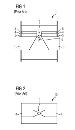
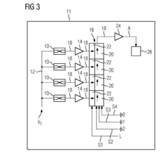
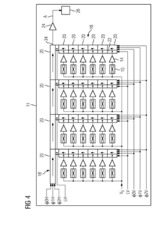
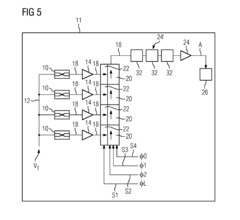
Sequencing Biopolymers
PatentActiveUS20160186254A1
Innovation
- The integration of image sensor technology principles with nanopore sequencing arrangements, utilizing shift registers like CCDs for parallel sequencing and noise-free charge transfer, enables simultaneous sequencing of multiple biopolymers with improved resolution and faster processing times.
Electronic device and method for producing the same
PatentInactiveUS20090075407A1
Innovation
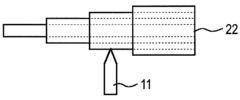
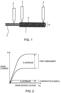
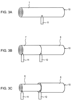
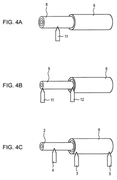
- The solution involves an electronic device structure where a semiconductive carbon nanotube layer is partially covered by a metallic carbon nanotube layer, with voltage-applying means controlling the electrical state of the semiconductive layer through a gate insulating layer, allowing for improved current modulation and reduced power consumption by ensuring uniform channel formation across the carbon nanotube layers.
Nanofabrication Techniques for Optimized Tunneling Structures
The fabrication of nanostructures optimized for quantum tunneling presents significant challenges due to the precise dimensional control required at the nanoscale. Current nanofabrication techniques for tunneling structures in nanoantennas have evolved considerably over the past decade, with several approaches demonstrating promising results for creating controlled tunneling junctions.
Electron beam lithography (EBL) remains the gold standard for creating precise tunneling gaps in nanoantenna structures, offering resolution down to 2-5 nm under optimal conditions. Recent advancements in EBL systems have incorporated proximity effect correction algorithms that compensate for electron scattering, enabling more consistent gap formation critical for tunneling measurements.
Focused ion beam (FIB) milling has emerged as a complementary technique, particularly valuable for creating three-dimensional tunneling structures. The latest gallium and helium ion beam systems can achieve sub-10 nm precision, though care must be taken to minimize ion implantation that could alter the electronic properties of the tunneling junction.
Self-assembly approaches represent a scalable alternative, with block copolymer lithography demonstrating particular promise for creating arrays of tunneling junctions with gaps as small as 3-7 nm. These methods benefit from parallel processing capabilities but suffer from higher variability in gap dimensions compared to direct-write techniques.
Atomic layer deposition (ALD) has become instrumental for precise control of tunneling barrier thickness. By depositing dielectric materials one atomic layer at a time, researchers can now engineer tunneling barriers with sub-angstrom precision, enabling systematic studies of tunneling efficacy as a function of barrier properties.
On-wire lithography and electrochemical methods have gained traction for creating axial heterostructures with embedded tunneling junctions. These approaches allow for the integration of different materials within a single nanostructure, creating complex tunneling architectures that would be difficult to achieve using traditional top-down methods.
Break junction techniques, while primarily used for measurement, have been adapted for fabrication of tunneling structures with exceptional control over gap dimensions. Mechanically controllable break junctions and electromigration-induced break junctions can create gaps tunable down to the sub-nanometer regime, though these approaches typically yield single devices rather than arrays.
The integration of in situ characterization during fabrication represents a significant advancement, with techniques such as transmission electron microscopy providing real-time feedback on gap formation. This has enabled iterative optimization of tunneling structures, substantially improving reproducibility and performance metrics in quantum tunneling experiments.
Quantum Computing Applications of Tunneling Nanoantennas
The integration of quantum tunneling phenomena in nanoantennas presents transformative opportunities for quantum computing architectures. Quantum tunneling nanoantennas can serve as novel interfaces between classical electronic systems and quantum processors, enabling more efficient quantum state preparation and measurement. These specialized nanoantennas leverage quantum mechanical effects to transmit and receive quantum information with minimal decoherence, addressing one of the fundamental challenges in quantum computing.
When implemented as quantum transducers, tunneling nanoantennas can facilitate the conversion between different quantum information carriers, such as photons, electrons, and phonons. This capability is particularly valuable for hybrid quantum computing systems that utilize multiple physical platforms to leverage their respective advantages. The tunneling mechanism provides a natural quantum channel that preserves coherence during these conversions, potentially increasing the fidelity of quantum operations.
In quantum error correction schemes, nanoantennas exploiting tunneling effects can enhance the detection of quantum errors by providing more sensitive measurement capabilities. The quantum tunneling process allows for non-destructive probing of quantum states, which is essential for implementing fault-tolerant quantum computing protocols. This application directly addresses the scalability challenges that currently limit practical quantum computing implementations.
For quantum memory applications, tunneling nanoantennas offer promising approaches to store and retrieve quantum information with high fidelity. The controlled tunneling process can be engineered to create stable quantum states with extended coherence times, potentially serving as quantum registers in future quantum processors. These memory elements could significantly reduce the resource requirements for quantum algorithms by maintaining quantum states between computational steps.
Additionally, quantum tunneling nanoantennas show potential for quantum networking applications, enabling the creation of entangled states between distant quantum processors. By precisely controlling the tunneling barriers, these nanoantennas can generate and manipulate entangled photon pairs, which are essential resources for quantum communication protocols and distributed quantum computing architectures.
The integration of these nanoantennas with conventional CMOS technology presents a pathway toward scalable quantum computing systems that can operate at higher temperatures than current superconducting approaches. This compatibility with existing semiconductor manufacturing processes could accelerate the commercial development of quantum computing technologies while reducing implementation costs.
Unlock deeper insights with Patsnap Eureka Quick Research — get a full tech report to explore trends and direct your research. Try now!
Generate Your Research Report Instantly with AI Agent
Supercharge your innovation with Patsnap Eureka AI Agent Platform!
