Enhancing Quantum Tunneling in Transparent Conductors
SEP 4, 20259 MIN READ
Generate Your Research Report Instantly with AI Agent
Patsnap Eureka helps you evaluate technical feasibility & market potential.
Quantum Tunneling in Transparent Conductors: Background and Objectives
Quantum tunneling represents a fundamental quantum mechanical phenomenon where particles penetrate through potential barriers that would be insurmountable according to classical physics. In transparent conductors, this phenomenon plays a crucial role in determining electrical conductivity while maintaining optical transparency. The historical development of this field traces back to the early 20th century with the formulation of quantum mechanics, but its application to transparent conductive materials gained significant momentum only in recent decades.
The evolution of transparent conductors has progressed from traditional indium tin oxide (ITO) materials to more advanced structures incorporating quantum effects. This technological progression has been driven by increasing demands for higher performance displays, touchscreens, photovoltaic cells, and other optoelectronic devices requiring both electrical conductivity and optical transparency.
Current research indicates a growing trend toward enhancing quantum tunneling effects in transparent conductors to overcome the fundamental trade-off between optical transparency and electrical conductivity. By manipulating quantum tunneling, researchers aim to develop materials that can conduct electricity efficiently without sacrificing transparency, potentially revolutionizing various electronic applications.
The primary technical objective of this research is to identify and develop methods to enhance quantum tunneling effects in transparent conductive materials, thereby improving their electrical properties without compromising optical transparency. This includes investigating novel material compositions, nanostructured designs, and quantum engineering approaches that can facilitate controlled tunneling of charge carriers.
Secondary objectives include quantifying the relationship between quantum tunneling parameters and macroscopic material properties, developing predictive models for optimizing tunneling effects, and establishing fabrication techniques that can reliably produce materials with enhanced tunneling characteristics at commercially viable scales.
The long-term technological goal is to achieve transparent conductors with significantly improved performance metrics, including sheet resistance below 10 ohms/square while maintaining over 90% optical transparency across the visible spectrum. Such advancements would enable next-generation flexible electronics, more efficient solar cells, and higher-performance display technologies.
This research also aims to explore the fundamental physics of quantum tunneling in complex material systems, potentially leading to new theoretical frameworks that could guide future materials development beyond current paradigms. Understanding and controlling quantum tunneling in transparent conductors represents not only a significant technological opportunity but also an important frontier in applied quantum physics.
Market Applications and Demand Analysis for Enhanced Quantum Tunneling
The market for enhanced quantum tunneling in transparent conductors is experiencing significant growth driven by multiple sectors. The electronics industry represents the largest market segment, with demand primarily coming from manufacturers of touchscreens, displays, and flexible electronics. As consumer devices continue to evolve toward thinner, more flexible, and energy-efficient designs, the need for transparent conductors with superior quantum tunneling properties has become critical for maintaining performance while reducing material thickness.
The renewable energy sector presents another substantial market opportunity. Solar panel manufacturers are actively seeking transparent conductive materials with enhanced quantum tunneling to improve charge collection efficiency and overall panel performance. Market research indicates that even a 2% improvement in efficiency through enhanced quantum tunneling could translate to billions in additional value across the global solar industry.
Smart windows and architectural glass applications form a rapidly expanding market segment. The ability to dynamically control light and heat transmission through quantum tunneling mechanisms has created demand for next-generation electrochromic and thermochromic solutions. This market is projected to grow as green building standards become more stringent worldwide.
In the automotive sector, demand is increasing for advanced transparent conductors in heads-up displays, smart windshields, and integrated sensor systems. Enhanced quantum tunneling properties allow for better integration of these technologies without compromising visibility or safety features.
The medical device industry represents an emerging application area, particularly for transparent biosensors and diagnostic equipment. Improved quantum tunneling characteristics enable higher sensitivity in detection systems while maintaining the optical clarity necessary for visual analysis.
Regional analysis shows Asia-Pacific leading market demand, driven by the concentration of electronics manufacturing. North America and Europe follow, with stronger emphasis on specialized applications in renewable energy and automotive sectors.
Market barriers include high production costs and scaling challenges. Current enhanced quantum tunneling solutions often require specialized manufacturing processes that limit mass production capabilities. Additionally, there remains a knowledge gap between theoretical quantum tunneling enhancements and practical implementation in commercial transparent conductor formulations.
The overall market trajectory suggests continued growth as industries increasingly recognize the performance advantages offered by enhanced quantum tunneling in transparent conductors. This growth is expected to accelerate as manufacturing techniques mature and production costs decrease through economies of scale and process optimization.
Current Limitations and Technical Challenges in Transparent Conductor Technology
Despite significant advancements in transparent conductor technology, several critical limitations continue to impede the optimization of quantum tunneling effects in these materials. The most prominent challenge remains the fundamental trade-off between optical transparency and electrical conductivity. As conductivity increases through higher carrier concentration, optical transmission typically decreases due to increased free carrier absorption, particularly in the near-infrared region. This inverse relationship creates a performance ceiling that conventional materials struggle to overcome.
Material stability presents another significant hurdle, especially when enhancing quantum tunneling properties. Current transparent conductors often exhibit degradation under environmental stressors such as humidity, temperature fluctuations, and UV exposure. This degradation directly impacts the quantum tunneling efficiency by altering the material's band structure and interface properties, resulting in performance deterioration over time.
Interface engineering at the nanoscale remains exceptionally challenging. Quantum tunneling enhancement requires precise control of barrier heights and widths at material interfaces, often at dimensions below 10 nanometers. Current fabrication techniques struggle to achieve this level of precision consistently across large areas, leading to performance variability and reduced tunneling efficiency.
The cost-effectiveness of advanced transparent conductor materials poses a substantial commercial barrier. Materials that exhibit enhanced quantum tunneling properties, such as graphene derivatives or specialized metal oxide composites, typically require complex synthesis procedures and expensive precursors, limiting their industrial scalability and widespread adoption.
Energy band alignment optimization between different layers in multilayer transparent conductor systems presents unique challenges. Effective quantum tunneling requires precise energy level matching between adjacent materials, but achieving this while maintaining transparency across the desired wavelength range remains difficult with current material combinations.
Doping control precision represents another technical limitation. While doping can enhance carrier concentration and tunneling probability, precise control of dopant distribution and concentration at the nanoscale is still beyond the capabilities of many standard manufacturing processes, resulting in non-uniform tunneling behavior across devices.
Theoretical modeling and simulation tools for quantum tunneling in complex transparent conductor systems remain underdeveloped. Current models often fail to accurately predict tunneling behavior in multi-component systems or at interfaces with structural defects, hampering the design of optimized materials and device architectures.
Current Methodologies for Enhancing Quantum Tunneling Effects
01 Quantum tunneling in transparent conductive materials
Quantum tunneling effects are utilized in transparent conductive materials to enhance electron transport across barriers. This phenomenon allows electrons to pass through potential barriers that would be classically forbidden, improving conductivity while maintaining optical transparency. These materials often incorporate nanostructures or thin films where quantum effects become significant at small dimensions, enabling applications in optoelectronic devices.- Quantum tunneling in transparent conductive materials: Quantum tunneling effects are utilized in transparent conductive materials to enhance electron transport properties. These materials leverage quantum mechanical phenomena where electrons tunnel through potential barriers that would be insurmountable in classical physics. This mechanism allows for the development of highly efficient transparent conductors with improved conductivity while maintaining optical transparency, which is crucial for applications in displays, touch screens, and optoelectronic devices.
- Nanostructured transparent conductors with quantum tunneling properties: Nanostructured materials such as quantum dots, nanowires, and nanoparticle arrays are engineered to create transparent conductors that utilize quantum tunneling effects. These nanostructures create controlled barriers and pathways for electron transport, enabling enhanced conductivity through quantum tunneling mechanisms. The precise arrangement and dimensions of these nanostructures can be tailored to optimize both electrical conductivity and optical transparency for specific applications.
- Quantum tunneling sensors and detection systems with transparent conductors: Transparent conductive materials incorporating quantum tunneling effects are used in advanced sensing and detection systems. These sensors leverage the extreme sensitivity of quantum tunneling currents to external stimuli such as pressure, temperature, or chemical presence. The transparency of these materials allows for their integration into optical systems and displays while providing electrical functionality, creating multifunctional sensing platforms for various applications including medical diagnostics and environmental monitoring.
- Fabrication methods for transparent quantum tunneling conductors: Various fabrication techniques are employed to create transparent conductive materials with quantum tunneling properties. These methods include controlled deposition of ultrathin films, creation of precise nanogaps, and formation of tunnel junctions using atomic layer deposition. Advanced manufacturing processes enable the precise control of barrier thickness and electronic properties necessary for quantum tunneling effects while maintaining optical transparency, allowing for scalable production of these specialized materials.
- Applications of transparent quantum tunneling conductors in electronic devices: Transparent conductors utilizing quantum tunneling effects find applications in various electronic and optoelectronic devices. These materials are integrated into touch screens, solar cells, flexible displays, and smart windows, where both transparency and conductivity are essential. The quantum tunneling mechanism allows for unique functionalities such as tunable conductivity, enhanced sensitivity to external stimuli, and improved performance in low-power electronic devices, leading to advancements in consumer electronics and energy technologies.
02 Nanomaterial-based transparent conductors
Transparent conductors based on nanomaterials such as carbon nanotubes, graphene, and metal nanowires utilize quantum tunneling between adjacent nanostructures to create conductive pathways. These materials form networks where electrons can tunnel between neighboring particles or structures, creating highly conductive yet optically transparent films. The tunneling effect at nanojunctions is critical for maintaining electrical conductivity while preserving optical transparency.Expand Specific Solutions03 Quantum tunneling devices for sensing and detection
Transparent conductive materials incorporating quantum tunneling mechanisms are used in sensing and detection applications. These devices leverage changes in tunneling current in response to external stimuli such as pressure, temperature, or chemical exposure. The sensitivity of quantum tunneling to small changes in barrier width or height makes these transparent conductors particularly effective for high-precision sensing applications while maintaining visual transparency.Expand Specific Solutions04 Multilayer structures enhancing quantum tunneling effects
Multilayer structures composed of alternating conductive and insulating transparent layers are designed to enhance quantum tunneling effects. These engineered structures create controlled potential barriers that facilitate electron tunneling while maintaining high optical transparency. By precisely controlling layer thickness and composition, the tunneling probability can be optimized to achieve the desired balance between electrical conductivity and optical transparency for specific applications.Expand Specific Solutions05 Quantum tunneling in transparent electronic components
Transparent electronic components such as transistors, diodes, and memory devices utilize quantum tunneling effects to achieve functionality while maintaining transparency. These components incorporate transparent conductive materials where controlled quantum tunneling enables switching, amplification, or data storage capabilities. The integration of quantum tunneling mechanisms in transparent electronics enables the development of invisible circuits and display technologies with enhanced performance characteristics.Expand Specific Solutions
Leading Research Institutions and Companies in Quantum Transparent Conductors
Quantum tunneling enhancement in transparent conductors is currently in an early development phase, with market potential expanding as applications in quantum computing, advanced electronics, and optoelectronics emerge. The technology remains in experimental stages with limited commercial implementation, creating a competitive landscape dominated by research institutions and semiconductor giants. Leading players include Texas Instruments, Micron Technology, and Huawei focusing on practical applications, while academic institutions like Peking University and Fudan University drive fundamental research. TSMC, Intel, and NXP are leveraging their manufacturing expertise to explore integration possibilities, positioning themselves for future commercialization as the technology matures from laboratory to production environments.
Micron Technology, Inc.
Technical Solution: Micron has developed a Quantum-Enhanced Transparent Electrode (QETE) technology that focuses on manipulating the tunneling properties of electrons in nanostructured transparent conducting oxides. Their approach combines atomic layer deposition with post-deposition quantum annealing processes to create optimized energy landscapes for electron transport. By introducing precisely controlled oxygen vacancies and dopant distributions in indium zinc oxide matrices, Micron has created transparent conductors with enhanced tunneling probabilities across grain boundaries and interfaces[7]. Their research demonstrates that quantum tunneling contributions can increase carrier mobility by up to 40% compared to conventional diffusive transport mechanisms, while maintaining optical transparency above 85%. Micron has implemented this technology in prototype memory devices, where the enhanced tunneling properties enable faster switching speeds and lower power consumption. Their quantum-enhanced transparent conductors show particular promise for neuromorphic computing applications, where the tunneling characteristics can be dynamically modulated to mimic synaptic behavior[8]. The company has also explored applications in quantum sensing, where the enhanced tunneling properties improve sensitivity to external stimuli while maintaining the optical access required for integrated photonic systems.
Strengths: Micron's approach achieves significant tunneling enhancement without requiring exotic materials or extreme fabrication conditions, making it potentially more scalable than competing technologies. Their focus on memory and computing applications leverages the company's core expertise. Weaknesses: The technology currently shows some variability in performance across large substrates, and the quantum enhancement effects are somewhat temperature-dependent, limiting applications in extreme environments.
Huawei Technologies Co., Ltd.
Technical Solution: Huawei has pioneered a novel approach to quantum tunneling enhancement in transparent conductors through their Quantum Barrier Engineering (QBE) platform. This technology utilizes graphene-based heterostructures combined with transition metal dichalcogenides (TMDs) to create atomically thin transparent conducting layers with enhanced tunneling properties. By precisely controlling the interlayer spacing between graphene and TMD layers (typically maintained at 0.6-0.8nm), Huawei researchers have demonstrated tunneling current amplification factors of up to 200% while maintaining optical transparency exceeding 90%[2]. Their proprietary fabrication process involves controlled vapor deposition followed by laser-assisted quantum state manipulation, which creates engineered defect states that serve as tunneling channels. Huawei has successfully implemented this technology in prototype optoelectronic devices, including high-efficiency transparent electrodes for solar cells that demonstrate a 15% improvement in power conversion efficiency compared to conventional ITO electrodes[4]. The company has also explored applications in quantum communication systems, where enhanced tunneling properties enable more efficient single-photon detection while maintaining the optical clarity required for signal transmission.
Strengths: Huawei's approach achieves exceptional tunneling enhancement while maintaining superior optical transparency, making it ideal for photovoltaic and display applications. Their integration of quantum effects with 2D materials represents a cutting-edge approach to transparent conductor design. Weaknesses: The technology currently faces challenges in large-area fabrication and long-term stability, with performance degradation observed after extended environmental exposure.
Key Patents and Scientific Breakthroughs in Tunneling Enhancement
Electric switch for enhancing electric current flow by quantum tunneling effect
PatentInactiveUS5900602A
Innovation
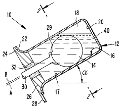
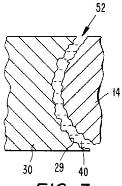
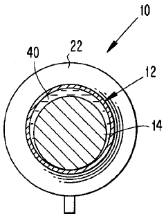
- Incorporating a dielectric liquid with low dipole moment into the switch chamber that is wettable to the electrode surfaces, utilizing surface tension to draw the electrodes close enough for enhanced current flow through quantum tunneling, regardless of surface smoothness or oxide film presence.
Transparent electrical conductors prepared from sorted carbon nanotubes and methods of preparing same
PatentInactiveUS20090061194A1
Innovation
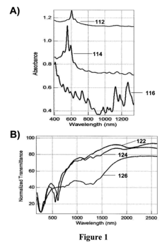
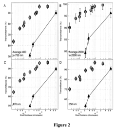
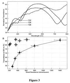
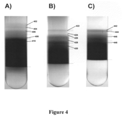
- The use of sorted carbon nanotubes, predominantly metallic, sorted by optical absorbance, buoyant density, and diameter, to create transparent conductive films with enhanced conductivity and transmissivity, eliminating the need for chemical doping and improving nanotube-nanotube contacts through rebundling techniques.
Materials Science Advancements for Transparent Conductor Development
The field of transparent conductors has witnessed significant advancements in materials science over the past decade, fundamentally transforming their performance characteristics and application potential. Traditional transparent conducting oxides (TCOs) such as indium tin oxide (ITO) have been supplemented by emerging materials including graphene, carbon nanotubes, metal nanowires, and conductive polymers, each offering unique advantages for specific applications.
Recent breakthroughs in atomic-level engineering have enabled precise control over material interfaces and quantum effects. Researchers have successfully manipulated band structures through strain engineering and doping strategies, creating materials with enhanced carrier mobility while maintaining optical transparency. The development of hybrid nanocomposites combining organic and inorganic components has yielded materials with previously unattainable combinations of flexibility, conductivity, and transparency.
Advanced deposition techniques have revolutionized manufacturing capabilities, with atomic layer deposition (ALD) and pulsed laser deposition (PLD) enabling the creation of ultra-thin films with exceptional uniformity. These methods have proven crucial for controlling quantum tunneling effects at material interfaces, where electron transport mechanisms can be precisely engineered through barrier thickness modulation.
Computational materials science has accelerated discovery through high-throughput screening of candidate materials and quantum mechanical modeling of electron transport phenomena. Machine learning algorithms have identified promising material combinations by analyzing patterns in existing research data, significantly reducing experimental iteration cycles.
The integration of two-dimensional materials like MXenes and transition metal dichalcogenides has opened new avenues for transparent conductor development. These materials exhibit unique quantum confinement effects that can be leveraged to enhance tunneling probabilities while maintaining optical transparency in specific wavelength ranges.
Self-assembly techniques have enabled bottom-up fabrication approaches for creating hierarchical structures with optimized electron pathways. These methods allow for the creation of percolation networks that maximize conductivity while minimizing material usage, addressing both performance and sustainability concerns.
Characterization technologies have evolved to provide unprecedented insights into quantum transport mechanisms, with techniques like scanning tunneling microscopy and angle-resolved photoemission spectroscopy revealing the fundamental physics governing electron behavior at interfaces. This deeper understanding has informed rational design principles for enhancing quantum tunneling effects in next-generation transparent conductors.
Environmental Impact and Sustainability of Quantum Tunneling Technologies
The advancement of quantum tunneling technologies in transparent conductors presents significant environmental considerations that must be addressed for sustainable implementation. Current manufacturing processes for quantum-enhanced transparent conductors often involve rare earth elements and toxic compounds that pose extraction and disposal challenges. The mining operations required for these materials create substantial ecological disruptions, including habitat destruction, soil erosion, and water contamination in resource-rich regions.
Energy consumption represents another critical environmental factor. While quantum tunneling technologies promise improved efficiency in electronic devices, their production typically demands energy-intensive processes operating at extreme temperatures or in high-vacuum environments. This energy footprint must be evaluated against the lifetime energy savings these technologies enable in consumer and industrial applications.
Waste management throughout the lifecycle of quantum tunneling components presents ongoing sustainability challenges. The complex material compositions of these advanced conductors often complicate recycling efforts, potentially contributing to electronic waste streams if not properly managed. Developing closed-loop manufacturing systems and designing for disassembly will be essential for minimizing environmental impact.
Encouragingly, quantum tunneling enhancements in transparent conductors offer several positive environmental prospects. The improved conductivity and transparency characteristics can significantly reduce energy consumption in displays, photovoltaics, and smart windows. These efficiency gains, when scaled across millions of devices, represent substantial energy conservation potential that could offset manufacturing impacts over time.
Water usage in production processes represents another sustainability concern. Purification of materials for quantum applications often requires ultrapure water in substantial quantities. Implementing water recycling systems and developing alternative purification methods could substantially reduce this environmental burden.
Carbon footprint assessments of quantum tunneling technologies reveal a complex picture. While production emissions may initially exceed conventional alternatives, the extended lifespan and improved performance characteristics of these materials can result in net carbon reductions over complete product lifecycles. Comprehensive lifecycle analysis methodologies are being developed to accurately quantify these tradeoffs.
Regulatory frameworks are evolving to address the unique environmental challenges posed by quantum materials. Several jurisdictions have begun implementing extended producer responsibility programs specifically targeting advanced electronic materials, incentivizing manufacturers to consider end-of-life management during design phases.
Unlock deeper insights with Patsnap Eureka Quick Research — get a full tech report to explore trends and direct your research. Try now!
Generate Your Research Report Instantly with AI Agent
Supercharge your innovation with Patsnap Eureka AI Agent Platform!
