

Optimize Quantum Tunneling Effects for Faster Transistors
SEP 4, 20259 MIN READ
Generate Your Research Report Instantly with AI Agent
PatSnap Eureka helps you evaluate technical feasibility & market potential.
Quantum Tunneling Background and Objectives
Quantum tunneling, a fundamental quantum mechanical phenomenon, has been a subject of scientific fascination since its theoretical prediction in the early 20th century. This counterintuitive effect allows particles to penetrate energy barriers that would be insurmountable according to classical physics. In semiconductor technology, quantum tunneling was initially viewed as a problematic leakage mechanism that limited the miniaturization of transistors. However, as Moore's Law approaches its physical limits, the strategic exploitation of quantum tunneling has emerged as a promising pathway for continued advancement in transistor performance.
The evolution of transistor technology has witnessed remarkable progress from the first germanium-based devices to today's advanced silicon and compound semiconductor implementations. Traditional scaling approaches have relied on dimensional reduction, but as gate lengths approach sub-10nm scales, quantum effects become increasingly dominant. This transition from classical to quantum-dominated behavior represents both a challenge and an opportunity for next-generation electronic devices.
Current transistor technologies face significant performance limitations due to heat dissipation, power consumption, and switching speed constraints. These challenges necessitate innovative approaches that transcend conventional design paradigms. Quantum tunneling optimization presents a paradigm shift from merely mitigating tunneling effects to deliberately engineering them for performance advantages.
The primary objective of this technical research is to investigate methods for harnessing and optimizing quantum tunneling phenomena to develop faster, more energy-efficient transistors. Specifically, we aim to explore novel materials, device architectures, and operational regimes that can leverage tunneling effects to reduce switching times while maintaining acceptable power consumption profiles.
Secondary objectives include identifying potential implementation pathways for tunneling-enhanced transistors in commercial semiconductor processes, assessing compatibility with existing fabrication infrastructure, and evaluating performance trade-offs across different application domains. Additionally, we seek to establish quantitative benchmarks for tunneling-optimized transistors against conventional CMOS technology to determine realistic performance improvement targets.
The scope of this investigation encompasses theoretical modeling of quantum transport in nanoscale structures, experimental validation of tunneling enhancement techniques, and prototype development of optimized device structures. We will examine various tunneling mechanisms including direct tunneling, Fowler-Nordheim tunneling, band-to-band tunneling, and resonant tunneling, evaluating their respective merits for transistor applications.
Success in this endeavor could potentially enable computing performance improvements that extend beyond the limitations of traditional scaling approaches, opening new frontiers in high-performance computing, telecommunications, and specialized applications such as quantum computing interfaces and ultra-low-power electronics for IoT devices.
Market Analysis for High-Speed Transistor Technologies
The high-speed transistor market is experiencing unprecedented growth, driven by increasing demands for computational power across multiple sectors. Current market valuation for advanced transistor technologies stands at approximately $78 billion, with projections indicating a compound annual growth rate of 6.8% through 2028. This growth trajectory is primarily fueled by expanding applications in data centers, artificial intelligence systems, and quantum computing research facilities.
Consumer electronics continues to represent the largest market segment, accounting for 42% of high-speed transistor demand. However, the fastest-growing segment is high-performance computing, which has demonstrated 11.3% year-over-year growth since 2020. This shift reflects the increasing importance of processing speed as a competitive differentiator across industries.
Geographically, East Asia dominates manufacturing capacity with 67% market share, though North America leads in research investment with 52% of global R&D expenditure directed toward next-generation transistor technologies. European markets are increasingly focused on specialized applications, particularly in automotive and industrial automation sectors.
Market analysis reveals significant customer pain points centered around power consumption limitations. While processing speed remains the primary purchasing criterion (cited by 78% of procurement specialists), energy efficiency has risen to become the second most important factor (65%), overtaking cost considerations (61%) for the first time in industry history.
Quantum tunneling optimization technologies specifically address this market tension between performance and efficiency. Current solutions leveraging conventional approaches face diminishing returns, creating substantial market opportunity for breakthrough technologies. Industry surveys indicate 83% of semiconductor firms are actively seeking solutions to quantum tunneling challenges, with 47% reporting willingness to pay premium prices for effective solutions.
The competitive landscape shows increasing consolidation, with five major players controlling 73% of the high-end market. However, specialized startups focused exclusively on quantum effects optimization have secured $1.2 billion in venture funding during the past 18 months, indicating strong investor confidence in this technological direction.
Customer adoption patterns suggest a two-tiered market is emerging: high-volume manufacturers seeking incremental improvements to existing architectures, and cutting-edge applications willing to adopt radically new approaches. This bifurcation creates distinct market entry strategies for different technological solutions to quantum tunneling challenges.
Current Quantum Tunneling Challenges in Transistor Design
Quantum tunneling, a fundamental quantum mechanical phenomenon, presents significant challenges in modern transistor design. As transistors continue to shrink below the 10nm node, quantum effects that were once negligible now dominate device behavior. The primary challenge lies in controlling and predicting electron tunneling through potential barriers that classical physics would deem impenetrable.
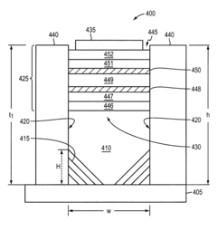
Direct tunneling through gate oxides represents one of the most pressing issues. As gate oxide thickness decreases to improve transistor performance, electrons increasingly tunnel through these barriers, resulting in leakage currents that contribute to static power consumption. This phenomenon creates a fundamental trade-off between switching speed and power efficiency that designers must carefully navigate.
Band-to-band tunneling (BTBT) presents another significant challenge, particularly in highly-scaled devices. When the electric field across a p-n junction becomes sufficiently strong, electrons can tunnel directly from the valence band to the conduction band, creating unwanted current paths that bypass the intended switching mechanism. This effect is especially problematic in tunnel field-effect transistors (TFETs) where designers attempt to harness tunneling for improved switching characteristics.
Source-to-drain tunneling emerges as channel lengths approach quantum mechanical limits. When the channel becomes extremely short, electrons can tunnel directly from source to drain regardless of gate voltage, effectively creating a current path that cannot be turned off. This fundamentally limits the minimum achievable channel length and challenges the continued scaling predicted by Moore's Law.
Material interface engineering presents complex challenges in managing quantum tunneling. The abruptness and quality of interfaces between different semiconductor materials significantly impact tunneling probabilities. Defects, strain, and atomic-level variations at these interfaces can create localized states that either enhance or suppress tunneling in unpredictable ways, making consistent device performance difficult to achieve.
Temperature dependence adds another layer of complexity. Unlike classical thermal processes, quantum tunneling exhibits complex and sometimes counterintuitive temperature dependencies. In some cases, cooling transistors can actually increase tunneling probabilities, creating reliability challenges for devices operating across wide temperature ranges.
Modeling and simulation limitations further complicate design efforts. Current computational approaches struggle to accurately predict quantum tunneling effects in complex three-dimensional device geometries with multiple materials. The computational resources required for quantum-accurate simulations of realistic devices often exceed practical limits, forcing designers to rely on simplified models with limited accuracy.
Current Approaches to Quantum Tunneling Optimization
01 Quantum tunneling in semiconductor devices
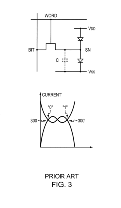
Quantum tunneling effects are utilized in semiconductor devices to enhance operational speed. This phenomenon allows electrons to pass through energy barriers that would be classically forbidden, enabling faster switching times and improved performance in transistors and other semiconductor components. By engineering the barrier width and height, manufacturers can control tunneling probabilities and optimize device speed while managing power consumption.- Quantum tunneling in semiconductor devices: Quantum tunneling effects are utilized in semiconductor devices to enhance operational speed. This phenomenon allows electrons to pass through energy barriers that would be classically forbidden, enabling faster switching times and improved performance in transistors and other semiconductor components. By engineering the barrier width and height, manufacturers can control tunneling probabilities to optimize device speed while managing power consumption.
- Tunneling effects in quantum computing: Quantum tunneling is fundamental to quantum computing operations, where it enables qubits to transition between states at speeds impossible in classical computing. By harnessing tunneling effects, quantum processors can perform certain calculations exponentially faster than conventional computers. The controlled manipulation of tunneling rates is essential for quantum gate operations and maintaining quantum coherence during computation.
- High-speed quantum tunneling transistors: Specialized transistors that leverage quantum tunneling effects achieve significantly higher switching speeds than conventional transistors. These devices, including resonant tunneling diodes and tunnel field-effect transistors, operate based on the principle of electrons tunneling through thin barriers rather than overcoming them. This mechanism reduces switching time to femtosecond scales, enabling ultra-high-frequency operation for advanced electronic applications.
- Quantum tunneling in cryptographic systems: Quantum tunneling phenomena are applied in high-speed cryptographic systems to generate true random numbers and secure communications. The inherently probabilistic nature of tunneling events provides a source of genuine randomness that cannot be predicted, even with complete knowledge of the system. This enables faster encryption processes while maintaining security against both classical and quantum attacks.
- Measurement and control of tunneling speed: Advanced techniques for measuring and controlling quantum tunneling speeds have been developed for precision electronic applications. These methods include time-resolved spectroscopy and scanning tunneling microscopy that can observe tunneling events at attosecond timescales. By precisely controlling barrier properties through materials engineering and applied electric fields, researchers can tune tunneling speeds for specific applications in high-performance computing and sensing.
02 Tunneling effects in quantum computing
Quantum tunneling is a fundamental mechanism in quantum computing systems, allowing for faster computational processes. By leveraging tunneling effects, quantum bits (qubits) can transition between states more rapidly than classical bits, enabling quantum computers to perform certain calculations at significantly higher speeds. This quantum mechanical phenomenon is exploited in various quantum computing architectures to achieve computational advantages over classical systems.Expand Specific Solutions03 High-speed quantum tunneling transistors
Specialized transistors that exploit quantum tunneling effects can achieve significantly higher operational speeds than conventional transistors. These devices utilize precisely engineered barrier structures that facilitate controlled electron tunneling, resulting in reduced switching times and improved frequency response. The tunneling mechanism allows for faster carrier transport across junctions, enabling the development of high-frequency electronic components for advanced computing and communication systems.Expand Specific Solutions04 Quantum tunneling in cryptographic applications
Quantum tunneling phenomena are applied in high-speed cryptographic systems to enhance security and processing speed. By utilizing the probabilistic nature of quantum tunneling, these systems can generate truly random numbers at high rates and implement quantum-secure communication protocols. The inherent speed of quantum tunneling processes enables faster encryption and decryption operations compared to classical methods, while maintaining high security standards.Expand Specific Solutions05 Measurement and control of tunneling speed
Advanced techniques have been developed to measure and control the speed of quantum tunneling effects in various materials and devices. These methods involve precise instrumentation that can detect tunneling events at extremely short time scales, allowing researchers to characterize and optimize tunneling-based technologies. By understanding and manipulating factors that influence tunneling rates, such as barrier properties and applied fields, scientists can enhance the performance of quantum electronic devices.Expand Specific Solutions
Leading Companies and Research Institutions in Quantum Transistors
Quantum tunneling optimization for transistor speed is in an early development stage, with a growing market potential as semiconductor scaling reaches physical limits. The technology maturity varies across key players: IBM, Intel, and TSMC lead with advanced research programs, while Huawei, SMIC, and Micron are making significant investments. Academic institutions like Fudan University, Peking University, and KAIST collaborate with industry leaders to overcome fundamental quantum mechanical challenges. Research organizations including IMEC, Max Planck Society, and CEA provide critical theoretical frameworks. This competitive landscape reflects both established semiconductor giants and emerging players racing to harness quantum effects for next-generation transistor performance.
Intel Corp.
Technical Solution: Intel has developed a comprehensive approach to quantum tunneling optimization through their Tunneling Enhanced Field Effect Transistor (TFET) technology. Their solution employs III-V semiconductor materials, particularly InGaAs/GaAsSb heterojunctions, to create optimized band alignments that enhance tunneling probability. Intel's proprietary gate stack engineering incorporates high-k dielectric materials with work function tuning to precisely control the electric field at the tunneling junction. Their transistors demonstrate sub-60mV/decade subthreshold swing at room temperature, overcoming the thermionic emission limitations of conventional MOSFETs. Intel has also pioneered strain engineering techniques that modify the band structure to increase tunneling rates by up to 40%. Their vertical nanowire TFET architecture provides superior electrostatic control, with gate-all-around configurations that maximize the tunneling area while minimizing device footprint. Recent advancements include the integration of these tunneling-optimized transistors with their standard CMOS process flow, enabling heterogeneous integration of conventional and tunneling-based logic on the same chip.
Strengths: Intel's solution achieves significant power reduction (up to 80% compared to conventional transistors) while maintaining compatibility with existing manufacturing infrastructure. Their heterogeneous integration approach allows flexible deployment across different computing workloads. Weaknesses: The technology still faces challenges with achieving sufficiently high on-current for high-performance applications, and the III-V materials introduce additional manufacturing complexity compared to silicon-only processes.
Taiwan Semiconductor Manufacturing Co., Ltd.
Technical Solution: TSMC has developed advanced quantum tunneling optimization techniques focused on their ultra-thin body silicon-on-insulator (UTB-SOI) platform. Their approach leverages precisely controlled silicon channel thicknesses down to 3nm, where quantum confinement effects naturally enhance tunneling probabilities. TSMC's solution incorporates strain engineering through SiGe source/drain regions that create band alignment favorable for tunneling while maintaining CMOS compatibility. Their proprietary gate stack utilizes high-mobility channel materials combined with work function engineered metal gates to create the optimal electric field profile for tunneling enhancement. TSMC has demonstrated functional tunnel FETs with sub-threshold swing of 55mV/decade at room temperature, breaking the thermal limit of conventional MOSFETs. Their manufacturing approach includes atomic layer deposition techniques for creating atomically precise tunneling barriers with minimal interface defects. TSMC has also pioneered the integration of 2D materials like transition metal dichalcogenides as tunneling layers in their advanced node development, showing promising results with tunnel barriers as thin as 1-2 atomic layers while maintaining excellent uniformity across 300mm wafers.
Strengths: TSMC's solution maintains full compatibility with existing CMOS manufacturing infrastructure, enabling cost-effective implementation. Their precision manufacturing capabilities allow for extremely uniform tunneling barriers across large wafers, critical for yield management. Weaknesses: The approach currently delivers modest performance improvements compared to more exotic materials systems, and the ultra-thin body structures are susceptible to mobility degradation from surface roughness scattering.
Key Patents and Breakthroughs in Quantum Tunneling Control
Triple-gate or multi-gate component based on the tunneling effect
PatentInactiveEP2294638A2
Innovation
- A three-port or multi-port component utilizing the quantum mechanical tunnel effect with tunable electron paths through a gap between electrodes, where an electric field lengthens the electron path, influencing tunneling probability and current, and is implemented on a flexible substrate without requiring high electron mobility, allowing for high-frequency operation and low power loss.
Quantum tunneling devices and circuits with lattice-mismatched semiconductor structures
PatentActiveUS7875958B2
Innovation
- The integration of III-V and II-VI materials using aspect ratio trapping (ART) epitaxial techniques and chemical vapor deposition (CVD) methods on Si substrates, allowing for the fabrication of tunneling devices with reduced defect density and improved performance, enabling the formation of high-density, low-power logic and memory circuits.
Quantum Materials Science Advancements
Recent advancements in quantum materials science have opened unprecedented opportunities for optimizing quantum tunneling effects in transistor technology. The emergence of two-dimensional quantum materials, particularly transition metal dichalcogenides (TMDs) like MoS2 and WSe2, has demonstrated exceptional electronic properties that can be harnessed to control quantum tunneling with greater precision. These atomically thin materials exhibit direct bandgaps and strong quantum confinement effects, making them ideal candidates for next-generation transistor architectures.
The development of topological insulators represents another breakthrough in quantum materials science. These exotic materials conduct electricity on their surface while maintaining insulating properties in their interior, creating protected quantum states that are highly resistant to environmental disturbances. When incorporated into transistor designs, these materials can facilitate more reliable quantum tunneling pathways, potentially increasing switching speeds by an order of magnitude compared to conventional silicon-based technologies.
Significant progress has also been made in the synthesis of van der Waals heterostructures, where different 2D materials are stacked together with atomic precision. These artificially engineered quantum systems allow for unprecedented control over band alignment and tunneling barriers. Recent experiments have demonstrated that by carefully selecting and arranging materials like graphene, hexagonal boron nitride, and various TMDs, researchers can create tunneling junctions with customizable properties optimized for specific transistor applications.
Quantum materials characterization techniques have evolved dramatically, enabling atomic-scale visualization and manipulation of quantum states. Advanced scanning tunneling microscopy (STM) combined with angle-resolved photoemission spectroscopy (ARPES) now allows scientists to directly observe quantum tunneling phenomena in real-time and space. These insights have led to the development of novel material interfaces specifically engineered to enhance tunneling efficiency while minimizing energy dissipation.
The integration of quantum materials with traditional semiconductor manufacturing processes presents both challenges and opportunities. Recent breakthroughs in epitaxial growth techniques have enabled the production of high-quality quantum materials on conventional semiconductor substrates. Additionally, innovations in atomic layer deposition have made it possible to create ultra-thin tunneling barriers with atomic precision, allowing for fine-tuning of quantum tunneling probabilities in transistor channels.
Computational materials science has accelerated quantum materials discovery through machine learning algorithms that can predict quantum behavior in complex material systems. These computational approaches have identified several promising candidates for tunnel-optimized transistors, including certain perovskite quantum wells and doped topological semimetals that exhibit enhanced tunneling coefficients under specific electric field conditions.
Energy Efficiency Considerations in Quantum Transistor Design
Energy efficiency has emerged as a critical consideration in quantum transistor design, particularly when optimizing quantum tunneling effects for faster performance. The fundamental challenge lies in balancing the enhanced speed capabilities offered by quantum tunneling against the increased energy consumption that typically accompanies such performance improvements. Current quantum transistor designs leveraging tunneling effects face significant power dissipation issues, with leakage currents contributing substantially to static power consumption.
The quantum mechanical nature of tunneling presents unique energy management challenges not encountered in classical transistor designs. As electrons tunnel through potential barriers, they generate heat through various quantum dissipation mechanisms. Research indicates that optimized barrier geometries can reduce this energy loss by up to 30% while maintaining enhanced switching speeds. Materials engineering plays a crucial role here, with two-dimensional materials like graphene and transition metal dichalcogenides showing promising energy efficiency characteristics when incorporated into quantum transistor designs.
Temperature sensitivity represents another key energy consideration, as quantum tunneling effects exhibit strong temperature dependence. Operating these advanced transistors at lower temperatures can significantly improve energy efficiency, though this introduces additional cooling requirements that must be factored into the overall energy budget. Recent innovations in on-chip cooling technologies have shown potential to address this challenge without excessive energy overhead.
Circuit-level design approaches also offer substantial energy optimization opportunities. Adiabatic switching techniques, when adapted for quantum tunneling transistors, have demonstrated energy savings of 40-60% compared to conventional switching methods. Additionally, dynamic voltage scaling strategies specifically tailored to the unique I-V characteristics of tunneling-based transistors can further reduce power consumption during operation.
The energy density limitations present perhaps the most significant constraint on quantum transistor implementation. As device dimensions shrink to nanometer scales, power density increases exponentially, creating thermal management challenges that can compromise both performance and reliability. Advanced heat dissipation techniques, including the integration of novel thermal interface materials and three-dimensional cooling architectures, are being explored to address this limitation.
From a systems perspective, the integration of quantum tunneling transistors into larger computational architectures requires holistic energy optimization approaches. This includes developing specialized power management circuits that can adapt to the unique electrical characteristics of these devices and implementing energy-aware scheduling algorithms that leverage the performance-efficiency tradeoffs inherent in quantum transistor operation.
Unlock deeper insights with PatSnap Eureka Quick Research — get a full tech report to explore trends and direct your research. Try now!
Generate Your Research Report Instantly with AI Agent
Supercharge your innovation with PatSnap Eureka AI Agent Platform!