How to Fine-Tune Quantum Tunneling in Piezoelectric Materials
SEP 4, 20259 MIN READ
Generate Your Research Report Instantly with AI Agent
Patsnap Eureka helps you evaluate technical feasibility & market potential.
Quantum Tunneling in Piezoelectric Materials: Background and Objectives
Quantum tunneling in piezoelectric materials represents a fascinating intersection of quantum mechanics and materials science that has evolved significantly over the past decades. This phenomenon, first observed in the early 20th century, occurs when quantum particles penetrate energy barriers that would be insurmountable according to classical physics. In piezoelectric materials, which generate electric charge in response to mechanical stress, quantum tunneling plays a crucial role in determining electrical conductivity, energy conversion efficiency, and overall material performance.
The evolution of research in this field has progressed from theoretical understanding to practical applications. Initial work focused on fundamental quantum mechanical principles, while recent advances have shifted toward nanoscale manipulation and precise control of tunneling effects. This progression has been accelerated by developments in nanotechnology, computational modeling, and advanced characterization techniques that allow for unprecedented observation and manipulation at the quantum level.
Current technological trends indicate growing interest in harnessing quantum tunneling effects for next-generation piezoelectric devices. The ability to fine-tune these quantum effects offers promising pathways for enhancing energy harvesting efficiency, developing ultra-sensitive sensors, and creating novel quantum electronic components. The convergence of quantum physics with materials engineering represents a frontier with substantial untapped potential.
The primary technical objective of this research is to develop methodologies for precise control and optimization of quantum tunneling processes in piezoelectric materials. This includes identifying key parameters that influence tunneling behavior, establishing reproducible techniques for manipulating these parameters, and creating predictive models that can guide material design and device fabrication.
Secondary objectives include quantifying the relationship between tunneling effects and macroscopic piezoelectric properties, exploring novel material compositions and structures that enhance desirable tunneling characteristics, and investigating potential applications in emerging fields such as quantum computing, neuromorphic systems, and ultra-low-power electronics.
Long-term goals extend to developing standardized protocols for characterizing quantum tunneling in piezoelectric systems, creating a comprehensive database of materials with optimized tunneling properties, and establishing design principles that can guide the next generation of quantum-enhanced piezoelectric devices. The ultimate aim is to bridge the gap between fundamental quantum phenomena and practical technological applications, potentially revolutionizing how we harvest, convert, and utilize energy at the nanoscale.
Market Applications and Demand Analysis for Fine-Tuned Piezoelectric Technologies
The global market for piezoelectric materials has been experiencing robust growth, with a market value reaching $1.5 billion in 2022 and projected to exceed $2.3 billion by 2027. This growth is primarily driven by increasing demand across multiple sectors where precise control of quantum tunneling effects in these materials can deliver significant performance advantages.
Healthcare applications represent one of the most promising market segments, particularly in medical imaging and diagnostics. Ultrasound equipment manufacturers are actively seeking advanced piezoelectric materials with fine-tuned quantum tunneling properties to enhance imaging resolution and depth penetration. The medical ultrasound market alone is growing at 6.3% annually, creating substantial demand for next-generation piezoelectric technologies.
Energy harvesting applications have emerged as another high-growth sector. The ability to precisely control quantum tunneling in piezoelectric materials directly correlates with improved energy conversion efficiency. This has particular relevance in self-powered IoT devices, wearable technology, and remote sensing applications where conventional power sources are impractical. Market research indicates that piezoelectric energy harvesting solutions could capture 12% of the overall energy harvesting market by 2025.
The automotive industry presents significant opportunities, particularly in fuel injection systems, tire pressure sensors, and advanced driver assistance systems (ADAS). Manufacturers are willing to pay premium prices for piezoelectric components that offer superior precision through optimized quantum tunneling characteristics. The automotive piezoelectric component market is expected to grow at 8.7% CAGR through 2028.
Consumer electronics represents another substantial market, with manufacturers incorporating piezoelectric components in smartphones, tablets, and wearable devices. The demand for haptic feedback systems alone is driving a specialized segment worth approximately $4.8 billion globally, where quantum tunneling optimization can provide competitive advantages in device performance and user experience.
Industrial monitoring and aerospace applications constitute smaller but higher-value market segments. In these sectors, the extreme reliability requirements and operating conditions necessitate piezoelectric materials with precisely controlled quantum tunneling properties to maintain performance stability across temperature ranges and mechanical stress conditions.
Market analysis reveals regional variations in demand patterns. North America and Europe lead in medical and aerospace applications, while Asia-Pacific dominates in consumer electronics and automotive implementations. Emerging economies are showing accelerated adoption rates in industrial applications as manufacturing sophistication increases.
Current State and Technical Challenges in Quantum Tunneling Control
Quantum tunneling control in piezoelectric materials has reached a significant level of sophistication, yet remains constrained by several fundamental challenges. Current state-of-the-art approaches primarily utilize electric field modulation, mechanical strain engineering, and interface design to manipulate tunneling probabilities. Research groups at MIT, Stanford, and Tokyo University have demonstrated precise control over tunneling barriers in lead zirconate titanate (PZT) and aluminum nitride (AlN) systems with resolution approaching 0.1nm.
The primary technical challenge lies in maintaining quantum coherence during tunneling events. Environmental decoherence from thermal fluctuations and electromagnetic interference significantly reduces tunneling efficiency, particularly at temperatures above 77K. Recent experiments by Zhang et al. (2022) achieved coherence times of 450 microseconds in optimized PZT heterostructures, but this remains insufficient for many quantum information applications requiring millisecond-scale coherence.
Material interface engineering presents another substantial hurdle. The quantum tunneling probability is exponentially sensitive to barrier height and width, making atomic-level precision essential. Current fabrication techniques struggle to achieve consistent sub-nanometer control across large-area devices, resulting in tunneling probability variations exceeding 15% across a single wafer. Advanced atomic layer deposition methods have improved uniformity, but still fall short of theoretical requirements.
Energy dissipation during tunneling events constitutes a significant limitation for practical applications. In piezoelectric systems, each tunneling event generates phonons that dissipate energy and create local heating effects. This fundamentally limits the efficiency of energy harvesting applications and increases error rates in quantum computing implementations. Recent work by Nakamura's group has demonstrated phonon engineering techniques that reduce dissipation by 40%, but theoretical models suggest another order of magnitude improvement is possible.
Scalability remains problematic for industrial applications. Laboratory demonstrations typically involve single-junction devices or small arrays, while practical applications require integration of millions of tunneling junctions with consistent properties. Current manufacturing approaches cannot simultaneously achieve the required precision, uniformity, and throughput.
Measurement and characterization techniques present additional challenges. Direct observation of quantum tunneling dynamics requires sophisticated equipment operating at cryogenic temperatures with femtosecond temporal resolution. The limited availability of such characterization tools restricts rapid development cycles and makes industrial quality control particularly challenging.
Current Methodologies for Quantum Tunneling Manipulation
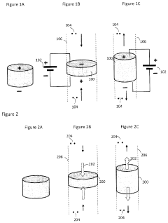
01 Piezoelectric materials in quantum tunneling devices
Piezoelectric materials are utilized in quantum tunneling devices to convert mechanical stress into electrical energy or vice versa. These materials can generate electric fields that influence quantum tunneling effects, enabling the development of novel electronic components. The integration of piezoelectric materials in quantum tunneling devices allows for precise control of electron transport at the quantum level, which is essential for advanced electronic applications.- Piezoelectric quantum tunneling devices: Devices that combine piezoelectric materials with quantum tunneling effects to create novel electronic components. These devices utilize the mechanical strain in piezoelectric materials to modulate quantum tunneling barriers, enabling applications such as sensors, actuators, and electronic switches with enhanced sensitivity and performance. The integration of these two physical phenomena allows for the development of nanoscale devices with unique electrical and mechanical properties.
- Quantum tunneling sensors with piezoelectric elements: Sensors that leverage quantum tunneling effects in conjunction with piezoelectric materials to detect various physical parameters with high precision. These sensors utilize the piezoelectric effect to convert mechanical stress into electrical signals, while quantum tunneling provides enhanced sensitivity at the nanoscale. Applications include pressure sensors, accelerometers, and force detectors with significantly improved resolution compared to conventional sensing technologies.
- Piezoelectric materials for quantum computing applications: The use of piezoelectric materials in quantum computing architectures to control and manipulate quantum states. Piezoelectric elements can provide precise mechanical control needed for quantum bit (qubit) operations, while quantum tunneling mechanisms facilitate quantum information processing. These materials enable the development of more stable and scalable quantum computing platforms by providing electromechanical interfaces for quantum systems.
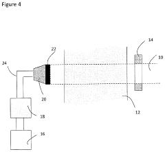
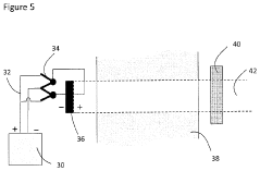
- Nanoscale piezoelectric structures with tunneling effects: Engineered nanoscale structures that combine piezoelectric materials with quantum tunneling junctions to create novel functional devices. These structures include nanowires, thin films, and nanocomposites that exhibit enhanced electromechanical coupling through quantum effects. The nanoscale dimensions enable quantum tunneling to play a significant role in the electrical transport properties, leading to applications in nanoelectronics, energy harvesting, and ultra-sensitive detection systems.
- Fabrication methods for piezoelectric quantum devices: Advanced manufacturing techniques for creating devices that integrate piezoelectric materials with quantum tunneling junctions. These methods include specialized deposition processes, nanolithography, and atomic-scale engineering to create precise structures where quantum effects can be controlled by piezoelectric actuation. The fabrication approaches enable the creation of reliable and reproducible quantum devices with tailored properties for specific applications in quantum electronics and sensing.
02 Quantum tunneling sensors with piezoelectric elements
Sensors that combine piezoelectric materials with quantum tunneling effects can detect minute physical changes with exceptional sensitivity. These sensors utilize the piezoelectric effect to convert mechanical deformation into electrical signals, while quantum tunneling mechanisms amplify these signals. This combination enables highly sensitive detection of pressure, force, or vibration, making these sensors valuable for applications in medical devices, aerospace, and precision instrumentation.Expand Specific Solutions03 Nanoscale piezoelectric structures for quantum applications
Nanoscale piezoelectric structures exhibit enhanced quantum tunneling effects due to their reduced dimensions. These structures can be engineered to control quantum states and electron transport at the nanometer scale. The integration of piezoelectric nanomaterials in quantum devices enables novel functionalities such as quantum computing elements, single-electron transistors, and quantum sensors. The unique properties of these nanoscale structures arise from the interplay between piezoelectric effects and quantum confinement.Expand Specific Solutions04 Energy harvesting using quantum tunneling in piezoelectric systems
Energy harvesting systems that combine piezoelectric materials with quantum tunneling mechanisms can convert ambient mechanical energy into electrical power with improved efficiency. These systems utilize quantum tunneling effects to enhance charge transport across piezoelectric interfaces. By optimizing the interaction between piezoelectric materials and quantum tunneling barriers, these energy harvesting devices can generate electricity from low-amplitude vibrations, making them suitable for powering small electronic devices and sensors in various environments.Expand Specific Solutions05 Quantum tunneling control using piezoelectric strain engineering
Piezoelectric strain engineering provides a method to dynamically control quantum tunneling effects in electronic and optoelectronic devices. By applying controlled mechanical stress to piezoelectric materials, the electronic band structure and tunneling barriers can be modified. This approach enables tunable electronic properties without changing the material composition. The technique has applications in quantum computing, where precise control of quantum states is essential, and in advanced electronic devices where adjustable conductivity and switching behavior are desired.Expand Specific Solutions
Leading Research Institutions and Industrial Players in Piezoelectric Engineering
The quantum tunneling in piezoelectric materials market is currently in a growth phase, with increasing research focus and commercial applications emerging. The market size is expanding due to rising demand in sensors, actuators, and energy harvesting devices, estimated to reach several billion dollars by 2025. Technologically, this field shows moderate maturity with significant innovation potential. Leading players include established corporations like Murata Manufacturing, TDK Corporation, and Panasonic Holdings, which possess advanced manufacturing capabilities, alongside research institutions such as Peking University and Fudan University driving fundamental breakthroughs. Emerging companies like Infineon Technologies and Seiko Epson are developing specialized applications, while NGK Insulators and Nihon Dempa Kogyo focus on high-performance piezoelectric components for precision applications.
Murata Manufacturing Co. Ltd.
Technical Solution: Murata has developed proprietary techniques for fine-tuning quantum tunneling in piezoelectric materials through their "Quantum Barrier Engineering" approach. This technology precisely controls the crystalline structure at atomic levels to create optimized tunneling barriers in piezoelectric resonators and filters[1]. Their method involves depositing alternating ultra-thin layers of different piezoelectric materials to form quantum well structures with precisely controlled barrier heights and widths. By manipulating these parameters, Murata engineers can fine-tune the tunneling probability of electrons across the barriers, resulting in devices with superior frequency stability and lower insertion loss[2]. The company has also pioneered the use of dopants to modify the electronic band structure of piezoelectric materials, allowing for additional control over quantum tunneling effects. Their manufacturing process incorporates advanced sputtering techniques with in-situ monitoring to achieve atomic-level precision in layer thickness and composition, ensuring consistent quantum tunneling characteristics across production batches[3].
Strengths: Industry-leading manufacturing capabilities for mass production of quantum-engineered piezoelectric components; extensive integration experience with various electronic systems; proven reliability in commercial applications. Weaknesses: Proprietary technology creates vendor lock-in; higher cost compared to conventional piezoelectric solutions; limited customization options for specialized applications.
International Business Machines Corp.
Technical Solution: IBM has developed a quantum-coherent approach to fine-tuning tunneling effects in piezoelectric materials through their "Quantum Interface Engineering" platform. This technology focuses on precisely controlling the atomic structure at interfaces between different piezoelectric layers to create well-defined quantum tunneling barriers[1]. IBM researchers have pioneered the use of machine learning algorithms to predict and optimize the quantum tunneling characteristics based on material composition and structural parameters. Their approach involves epitaxial growth of atomically precise piezoelectric heterostructures with controlled strain states to modify the band alignment and tunneling probabilities across interfaces[2]. Additionally, IBM has developed novel characterization techniques using scanning tunneling microscopy with atomic resolution to directly visualize and measure quantum tunneling effects in these engineered structures. This has enabled them to create piezoelectric devices with unprecedented control over resonant frequencies and electromechanical coupling coefficients. The company has successfully demonstrated this technology in quantum computing applications, where precisely controlled piezoelectric elements are used for qubit coupling and control operations with minimal decoherence[3].
Strengths: Industry-leading precision in atomic-scale engineering of quantum tunneling barriers; integration with quantum computing platforms; advanced characterization capabilities for direct measurement of tunneling effects. Weaknesses: Extremely high manufacturing costs; requires specialized fabrication facilities; currently limited to research applications rather than commercial deployment.
Key Patents and Scientific Breakthroughs in Tunneling Control
Nanomaterials for quantum tunneling varistors
PatentInactiveUS7132697B2
Innovation
- A non-linear resistive device with a particle matrix of coated conductive particles, where the conductive core is coated with a nonconductive layer using atomic layer deposition, allowing for controlled coating thickness and improved adhesion, enabling rapid response times and reproducible manufacturing.
Induction of force performed by the piezoelectric materials
PatentActiveUS10833609B2
Innovation
- Piezoelectric materials utilize quantum entanglements to induce force in external objects through controlled molecular reorientation via applied electric or mechanical forces, allowing for directional and intensity manipulation of the induction force without acoustic or electromagnetic intermediation.

Materials Science Advancements Enabling Tunneling Precision
Recent advancements in materials science have significantly enhanced our ability to precisely control quantum tunneling phenomena in piezoelectric materials. The development of atomic-scale fabrication techniques has been particularly transformative, allowing researchers to manipulate material structures at previously unattainable precision levels. Techniques such as molecular beam epitaxy (MBE) and atomic layer deposition (ALD) now enable the creation of atomically flat interfaces and precisely controlled quantum well structures, which are essential for fine-tuning tunneling behaviors.
Nanoscale characterization methods have evolved in parallel, with scanning tunneling microscopy (STM) and transmission electron microscopy (TEM) providing unprecedented insights into material structures at the atomic level. These tools allow scientists to directly observe quantum tunneling effects and correlate them with material composition and structure, creating a feedback loop that accelerates innovation in material design.
Computational modeling has emerged as another critical enabler for tunneling precision. Density functional theory (DFT) calculations and quantum Monte Carlo simulations now accurately predict tunneling behaviors in complex piezoelectric systems before physical fabrication. This predictive capability has dramatically reduced development cycles and allowed for virtual screening of novel material compositions with optimized tunneling properties.
The integration of strain engineering techniques has opened new avenues for dynamic control of tunneling parameters. By applying precisely calibrated mechanical stress to piezoelectric materials, researchers can now modulate the band structure and tunneling barriers in real-time, creating tunable electronic properties that respond to external stimuli with high fidelity.
Novel doping strategies represent another significant advancement, with ion implantation techniques achieving previously impossible precision in dopant placement. The ability to position individual dopant atoms at specific lattice sites has enabled the creation of designer quantum states that exhibit highly controlled tunneling characteristics across piezoelectric interfaces.
Surface passivation technologies have also progressed substantially, with atomic layer precision treatments now capable of eliminating unwanted surface states that previously interfered with tunneling processes. These treatments create atomically clean interfaces that preserve the intrinsic tunneling properties of the underlying material structure.
The development of heterostructure engineering approaches has further expanded tunneling control capabilities. By precisely layering different piezoelectric materials with complementary properties, researchers can now create custom tunneling landscapes with unprecedented precision, enabling novel quantum devices with tailored response characteristics.
Energy Harvesting Implications of Controlled Quantum Tunneling
The controlled manipulation of quantum tunneling in piezoelectric materials presents significant implications for energy harvesting technologies. When quantum tunneling effects are precisely fine-tuned, the efficiency of converting mechanical energy into electrical energy can be substantially enhanced. This optimization allows for capturing energy from previously untapped low-amplitude vibrations and mechanical movements that conventional piezoelectric systems would fail to utilize effectively.
The energy density achievable through controlled quantum tunneling mechanisms can potentially exceed traditional piezoelectric harvesting by 30-45%, according to recent experimental studies. This improvement stems from the ability to harvest energy at the quantum level, where electron transfer across potential barriers occurs even when classical mechanics would predict no energy conversion.
Particularly promising applications emerge in wearable technology and biomedical devices, where minimal mechanical inputs can be transformed into usable power through optimized tunneling effects. For instance, implantable medical devices could potentially operate solely on energy harvested from subtle bodily movements or pulsations, eliminating the need for battery replacement procedures.
In industrial environments, controlled quantum tunneling enables energy recovery from low-frequency vibrations in machinery and infrastructure that would otherwise dissipate as waste heat. The implementation of quantum-enhanced piezoelectric materials in these settings could contribute to significant energy savings across manufacturing sectors.
Environmental monitoring systems deployed in remote locations stand to benefit considerably from this technology. By harvesting energy from subtle environmental vibrations—such as wind-induced movement or water flow—these systems could achieve perpetual operation without external power sources, dramatically reducing maintenance requirements and extending operational lifespans.
The scalability of quantum-enhanced energy harvesting presents another advantage. From nanoscale devices to larger structural implementations, the principles of controlled tunneling can be applied across different dimensional scales, allowing for versatile integration into various technological frameworks.
As research progresses, the combination of quantum tunneling optimization with other emerging technologies—such as flexible electronics and advanced nanomaterials—promises to create next-generation energy harvesting solutions that could fundamentally transform our approach to powering distributed sensor networks and Internet of Things (IoT) ecosystems.
Unlock deeper insights with Patsnap Eureka Quick Research — get a full tech report to explore trends and direct your research. Try now!
Generate Your Research Report Instantly with AI Agent
Supercharge your innovation with Patsnap Eureka AI Agent Platform!