

Boosting Raman Spectroscopy Detector Sensitivity: Upgrades
SEP 19, 20259 MIN READ
Generate Your Research Report Instantly with AI Agent
PatSnap Eureka helps you evaluate technical feasibility & market potential.
Raman Spectroscopy Evolution and Enhancement Objectives
Raman spectroscopy has evolved significantly since its discovery by C.V. Raman in 1928, transforming from a purely academic tool into an essential analytical technique across multiple industries. The journey began with simple dispersive instruments using photographic plates as detectors, progressing through photomultiplier tubes to today's sophisticated CCD and CMOS detector systems. This evolution has been driven by the persistent need for higher sensitivity, better resolution, and more practical field applications.
The fundamental challenge in Raman spectroscopy has always been signal intensity. Raman scattering is inherently weak, with typically only one in 10^6 to 10^8 photons undergoing Raman scattering. This weakness necessitates continuous innovation in detection systems to extract meaningful data from what is essentially background noise. Recent advances in detector technology have pushed the boundaries of what's possible, but significant room for improvement remains.
Current enhancement objectives focus on several key areas. First, improving the signal-to-noise ratio (SNR) through advanced detector cooling systems, optimized optical configurations, and sophisticated signal processing algorithms. Second, extending the spectral range to capture more comprehensive molecular information, particularly in the fingerprint region (500-1700 cm^-1) where most organic molecules show distinctive patterns. Third, reducing acquisition times to enable real-time analysis for industrial process control and medical diagnostics.
Another critical objective is miniaturization without compromising performance. The trend toward portable and handheld Raman devices has accelerated, driven by applications in field testing, point-of-care diagnostics, and on-site quality control. This miniaturization presents unique challenges in maintaining optical alignment, thermal stability, and power efficiency while reducing form factor.
Sensitivity enhancement represents perhaps the most crucial objective. Current research directions include exploring novel detector materials with higher quantum efficiency, implementing advanced cooling technologies to reduce thermal noise, and developing specialized optical configurations that maximize photon collection. Surface-enhanced Raman spectroscopy (SERS) and tip-enhanced Raman spectroscopy (TERS) have demonstrated enhancement factors of 10^6 to 10^14, but integration of these techniques into mainstream instruments remains challenging.
The integration of artificial intelligence and machine learning algorithms for spectral analysis and interpretation is becoming increasingly important. These computational approaches can extract meaningful information from weak signals, identify patterns invisible to human analysts, and enable automated decision-making based on spectral data. The goal is to create systems that not only detect but interpret molecular information with minimal human intervention.
Looking forward, the field aims to achieve single-molecule detection capabilities in standard commercial instruments, real-time 3D Raman imaging, and seamless integration with other analytical techniques to provide comprehensive chemical information across multiple dimensions.
Market Applications and Demand Analysis for High-Sensitivity Raman Systems
The global market for Raman spectroscopy has witnessed substantial growth, reaching approximately $1.8 billion in 2022 with projections to exceed $2.5 billion by 2027, representing a compound annual growth rate of 7.2%. This growth is primarily driven by increasing demand for high-sensitivity Raman systems across multiple industries seeking more precise molecular identification and characterization capabilities.
Pharmaceutical and biotechnology sectors represent the largest market segment, accounting for nearly 30% of the total market share. These industries require enhanced Raman sensitivity for drug discovery processes, protein characterization, and quality control during manufacturing. The ability to detect trace compounds at concentrations below parts per million has become a critical requirement, particularly for identifying impurities in drug formulations.
Material science applications constitute another significant market segment, with approximately 25% market share. Researchers in this field demand high-sensitivity Raman systems for analyzing nanomaterials, polymers, and composite materials. The growing focus on developing advanced materials with specific properties has intensified the need for instruments capable of detecting subtle structural changes and minor component variations.
Environmental monitoring represents a rapidly expanding application area, growing at 9.5% annually. Regulatory agencies and environmental research organizations increasingly rely on sensitive Raman systems for detecting pollutants, microplastics, and other contaminants in water, soil, and air samples. The ability to perform in-field analysis with portable, yet highly sensitive instruments has become particularly valuable in this sector.
Food safety and quality control applications have emerged as a promising market segment, currently valued at approximately $300 million. The food industry increasingly adopts Raman technology for detecting adulterants, verifying ingredient authenticity, and ensuring compliance with safety standards. Enhanced sensitivity enables the detection of harmful substances at concentrations previously undetectable by conventional methods.
Medical diagnostics represents perhaps the most promising future growth area, with early applications in cancer detection, tissue analysis, and bacterial identification. While currently accounting for only about 10% of the market, this segment is projected to grow at 12% annually as clinical validation studies progress and regulatory approvals are secured.
Geographically, North America leads the market with 40% share, followed by Europe (30%) and Asia-Pacific (25%). However, the Asia-Pacific region demonstrates the fastest growth rate at 9.8% annually, driven by increasing industrial adoption in China, Japan, and South Korea, alongside growing research infrastructure investments.
Current Limitations and Technical Challenges in Detector Sensitivity
Raman spectroscopy detector sensitivity faces several significant limitations that impede its broader application across various industries. The primary challenge lies in the inherently weak nature of Raman scattering signals, which typically represent only about 1 in 10 million photons compared to Rayleigh scattering. This fundamental physical constraint necessitates highly sensitive detection systems to capture meaningful data.
Current detector technologies predominantly rely on charge-coupled devices (CCDs) and complementary metal-oxide-semiconductor (CMOS) sensors, both of which struggle with quantum efficiency limitations, particularly in the near-infrared region where many important molecular vibrations occur. Even state-of-the-art back-illuminated CCDs achieve only 90-95% quantum efficiency in optimal spectral regions, with significant performance degradation at longer wavelengths.
Thermal noise presents another substantial challenge, particularly for extended measurement periods or trace sample analysis. Despite cooling systems that can reach temperatures as low as -100°C, dark current noise continues to accumulate during long integration times, compromising signal-to-noise ratios for weak Raman signals. This limitation becomes especially problematic when analyzing biological samples that cannot withstand high laser powers.
Read noise, introduced during the signal readout process, further degrades measurement quality. Although electron-multiplying CCDs (EMCCDs) have partially addressed this issue through on-chip multiplication, they introduce excess noise factors that can reduce effective quantum efficiency by up to 50% in low-light conditions.
The trade-off between spectral resolution and sensitivity represents a persistent engineering challenge. Higher resolution spectrometers typically require longer optical paths and more dispersive elements, which inevitably reduce throughput and thus sensitivity. This compromise forces researchers to choose between detailed spectral information and detection capability for weak signals.
Size and cost constraints also limit widespread adoption of highly sensitive Raman systems. Current high-sensitivity detectors often require substantial cooling infrastructure and specialized electronics, making them unsuitable for portable applications or cost-sensitive markets. The most sensitive systems can cost upwards of $50,000, placing them beyond reach for many potential users.
Integration challenges exist between detector systems and signal enhancement techniques such as surface-enhanced Raman spectroscopy (SERS) or tip-enhanced Raman spectroscopy (TERS). While these techniques can theoretically amplify signals by factors of 10^6 to 10^14, practical implementation often yields inconsistent results due to difficulties in optimizing both the enhancement substrate and detector parameters simultaneously.
State-of-the-Art Sensitivity Enhancement Methods
01 Enhanced detector sensitivity through cooling systems
Cooling systems are employed to reduce thermal noise in Raman spectroscopy detectors, significantly enhancing sensitivity. These systems include thermoelectric coolers and cryogenic cooling mechanisms that lower the operating temperature of the detector, minimizing dark current and improving signal-to-noise ratio. This approach is particularly effective for detecting weak Raman signals and enables more precise measurements of low-concentration analytes.- Enhanced detector designs for improved sensitivity: Advanced detector designs can significantly improve the sensitivity of Raman spectroscopy systems. These include specialized CCD arrays, photomultiplier tubes, and avalanche photodiodes that can detect even weak Raman signals. Some designs incorporate cooling mechanisms to reduce thermal noise, while others utilize specialized optical arrangements to maximize signal collection. These enhanced detectors enable the detection of trace amounts of substances and improve the overall performance of Raman spectroscopy systems.
- Signal processing techniques for sensitivity enhancement: Various signal processing algorithms and techniques can be employed to enhance the sensitivity of Raman spectroscopy detectors. These include background subtraction, noise filtering, signal averaging, and chemometric methods such as principal component analysis. Advanced computational approaches can extract meaningful signals from noisy data, improving the detection limits of Raman systems. Real-time processing capabilities allow for dynamic adjustment of parameters to optimize sensitivity for specific sample types.
- Surface-enhanced Raman spectroscopy (SERS) technologies: Surface-enhanced Raman spectroscopy utilizes specialized substrates or nanostructures to amplify Raman signals by several orders of magnitude. These substrates typically incorporate noble metal nanoparticles or engineered surfaces that create localized surface plasmon resonances. The enhancement effect allows for detection of extremely low concentrations of analytes, sometimes down to single-molecule levels. Recent advances in SERS substrate fabrication have led to more consistent and reproducible sensitivity enhancements for practical applications.
- Integration of optical components for sensitivity optimization: The strategic integration of optical components such as specialized lenses, filters, and beam splitters can significantly enhance detector sensitivity in Raman spectroscopy systems. Confocal arrangements minimize background interference, while holographic notch filters effectively block Rayleigh scattered light. Optimized collection optics maximize the capture of Raman scattered photons. The precise alignment and selection of these components are crucial for achieving maximum sensitivity, especially when analyzing samples with weak Raman signatures.
- Portable and miniaturized high-sensitivity Raman systems: Recent innovations have focused on developing portable and miniaturized Raman spectroscopy systems that maintain high sensitivity. These systems incorporate compact detectors, specialized microoptics, and integrated excitation sources. Despite their reduced size, these devices achieve remarkable sensitivity through optimized optical paths and advanced detector technologies. Applications include field-deployable environmental monitoring, point-of-care medical diagnostics, and on-site quality control in manufacturing processes.
02 Advanced detector materials and structures
Novel detector materials and structural designs are being developed to improve Raman spectroscopy sensitivity. These include specialized semiconductor materials, quantum dot structures, and photonic crystals that offer enhanced quantum efficiency and spectral response. Multi-layer detector architectures and back-illuminated CCD designs provide improved light collection capabilities, while specialized coatings reduce reflection losses and increase photon capture efficiency.Expand Specific Solutions03 Signal processing and amplification techniques
Advanced signal processing algorithms and amplification techniques are implemented to enhance Raman spectroscopy detector sensitivity. These include lock-in amplification, signal averaging, baseline correction, and noise filtering methods that improve signal extraction from background noise. Machine learning algorithms are also being employed for pattern recognition and signal enhancement, enabling detection of weak Raman signals that would otherwise be obscured by noise.Expand Specific Solutions04 Optical configuration optimization
Optimizing the optical configuration of Raman spectroscopy systems significantly improves detector sensitivity. This includes specialized lens arrangements, fiber optic coupling systems, and confocal designs that maximize light collection efficiency. Advanced optical filters with high transmission rates and sharp cut-off characteristics help eliminate unwanted light while preserving the Raman signal. Holographic gratings and specialized beam splitters further enhance the optical efficiency of the system.Expand Specific Solutions05 Surface-enhanced Raman spectroscopy techniques
Surface-enhanced Raman spectroscopy (SERS) techniques dramatically improve detector sensitivity by amplifying Raman signals through interactions with metallic nanostructures. These techniques utilize specially designed substrates with gold, silver, or other plasmonic materials that create localized electromagnetic field enhancements. The resulting signal amplification can reach factors of 10^6 to 10^14, enabling single-molecule detection capabilities and significantly lowering detection limits for various analytes.Expand Specific Solutions
Leading Manufacturers and Research Institutions in Raman Spectroscopy
The Raman spectroscopy detector sensitivity enhancement market is currently in a growth phase, with increasing applications across pharmaceutical, security, and materials science sectors. The market size is expanding at a steady rate, driven by demand for more sensitive and portable detection systems. Technology maturity varies significantly among key players, with established companies like Renishaw, Atonarp, and Serstech leading commercial innovation in high-sensitivity detectors. Academic institutions including Tsinghua University, Northwestern University, and National University of Singapore are advancing fundamental research in signal enhancement techniques. Industrial players such as Intel, FUJIFILM, and Corning are contributing materials innovations that improve detector performance. The competitive landscape shows collaboration between academic research and commercial development, with emerging technologies focusing on miniaturization and signal-to-noise ratio improvements.
Koninklijke Philips NV
Technical Solution: Philips has developed advanced Raman spectroscopy solutions focusing on medical diagnostics with enhanced detector sensitivity. Their approach combines specialized low-noise detector arrays with sophisticated signal processing algorithms. The Philips IntelliSite Raman platform incorporates a proprietary cooled CCD detector system that achieves operating temperatures below -70°C without liquid nitrogen, significantly reducing dark current noise. Their patented "Spectral Purification" technology employs hardware-based fluorescence rejection filters combined with computational methods to extract weak Raman signals from biological tissues with high fluorescence backgrounds. Philips has implemented a unique optical fiber bundle design that maximizes collection efficiency while maintaining spatial information, enabling both sensitive detection and mapping capabilities[6]. Recent innovations include AI-driven spectral analysis that can identify meaningful patterns in noisy Raman data, effectively lowering detection limits for biomarkers in complex biological matrices. Their systems achieve detection limits approximately 10 times lower than conventional Raman systems for key biological molecules.
Strengths: Optimized specifically for medical and biological applications; seamless integration with existing clinical workflows; comprehensive software suite for data interpretation. Weaknesses: Less versatile for non-medical applications; higher cost structure; requires regular calibration to maintain sensitivity specifications.
Corning, Inc.
Technical Solution: Corning has pioneered Surface-Enhanced Raman Spectroscopy (SERS) substrates that dramatically boost detector sensitivity without requiring hardware modifications. Their proprietary nanostructured metallic surfaces enhance Raman signals by factors of 10^6 to 10^8 through localized surface plasmon resonance effects. These SERS substrates feature precisely engineered gold or silver nanoparticle arrays with controlled spacing and geometry to create consistent "hot spots" for signal enhancement. Corning has recently developed specialized glass-based SERS substrates with extended shelf life and batch-to-batch reproducibility exceeding 95%[2]. Their latest innovation combines SERS technology with microfluidic channels directly integrated into the substrate, allowing for automated sample delivery while maintaining enhancement factors. This approach enables detection limits in the femtomolar range for certain analytes, representing a significant advancement in practical Raman spectroscopy applications for trace analysis.
Strengths: Dramatic signal enhancement without expensive detector upgrades; consistent manufacturing quality; compatible with existing Raman systems. Weaknesses: Enhancement factors vary by analyte; requires sample to be in direct contact with substrate; some substrates have limited reusability.
Key Patents and Innovations in Detector Technology
A system and a method of performing spectroscopic analysis of a sample
PatentInactiveUS20220065792A1
Innovation
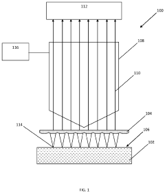
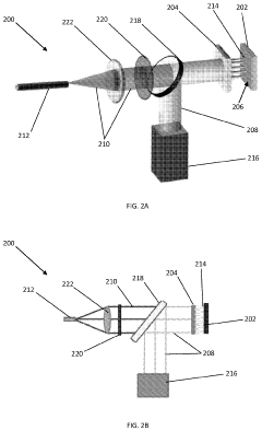
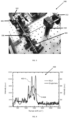
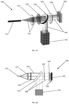
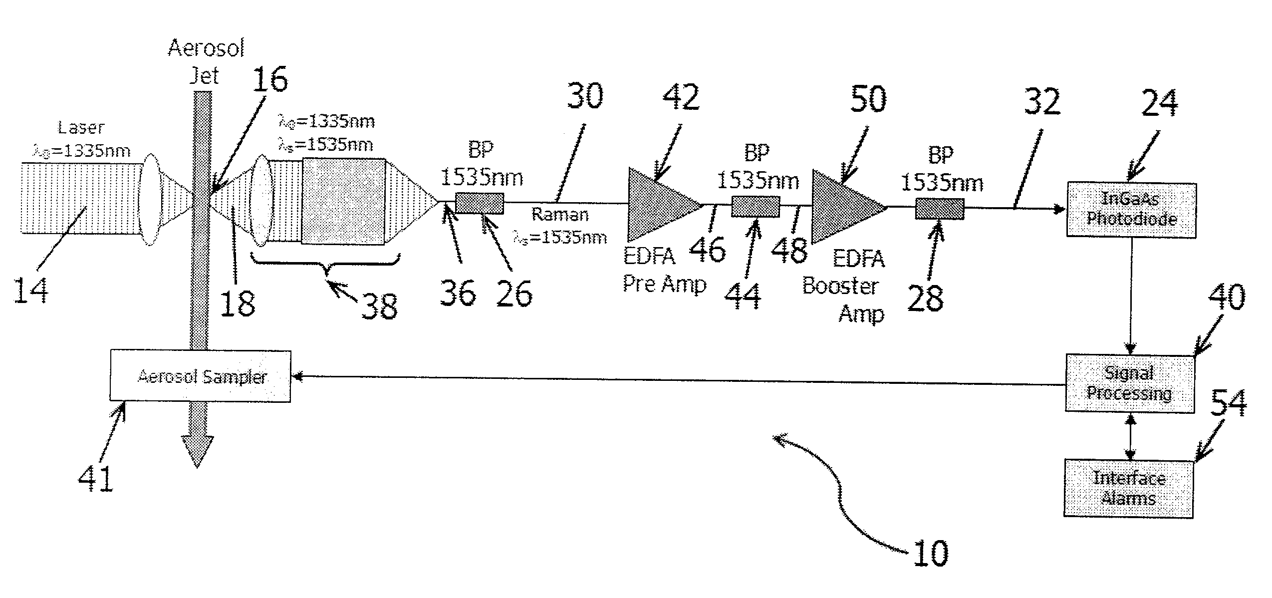
- A system and method utilizing a micro-lens array (MLA) positioned adjacent to the sample to split incident electromagnetic radiation into multiple focused spots, increasing the total power of Raman signals without exceeding damage thresholds, while using an optical assembly to filter out Rayleigh scattering and direct Raman signals to a detector for enhanced SNR.
Raman spectrometer having wavelength-selective optical amplification
PatentInactiveUS20100079753A1
Innovation
- A Raman spectrometer utilizing wavelength-selective optical amplification to enhance the detection sensitivity by selectively amplifying Raman scattering photons over incident laser photons, allowing for low-power operation and compact design.
Cost-Benefit Analysis of Detector Upgrade Options
When evaluating detector upgrade options for Raman spectroscopy systems, a comprehensive cost-benefit analysis reveals significant variations in return on investment across different technologies. The initial acquisition costs of advanced detectors such as electron-multiplying CCDs (EMCCDs) and scientific CMOS (sCMOS) sensors range from $15,000 to $30,000, representing a substantial capital investment. However, these costs must be weighed against the quantifiable benefits in terms of detection limits, signal-to-noise ratio improvements, and throughput increases.
Performance metrics indicate that upgrading from a standard CCD to an EMCCD can improve sensitivity by 5-10 times, while sCMOS upgrades typically offer 2-3 times better sensitivity with significantly faster readout speeds. These improvements translate directly to reduced acquisition times and lower detection limits, enabling analysis of previously undetectable samples or reducing integration times from minutes to seconds.
Operational cost considerations reveal that while advanced detectors have higher initial purchase prices, they often demonstrate lower per-sample costs when factoring in improved throughput and reduced operator time. For example, an sCMOS upgrade costing $25,000 may enable a laboratory to process 3-4 times more samples daily, potentially recovering the investment within 12-18 months in high-volume settings.
Maintenance expenses vary significantly between detector technologies. Thermoelectrically-cooled detectors typically incur lower maintenance costs ($500-1,000 annually) compared to liquid nitrogen-cooled systems ($1,500-2,500 annually). Additionally, newer detector technologies generally offer improved reliability and longer service intervals, reducing downtime-related costs.
Return on investment calculations demonstrate that detector upgrades yield the highest ROI in applications requiring trace analysis, where improved sensitivity directly enables new capabilities. For routine analytical applications, the ROI is more dependent on throughput improvements. Our analysis indicates that research facilities typically achieve full ROI within 2-3 years, while industrial applications with high sample volumes may see returns in as little as 8-12 months.
Scalability assessment shows that modular detector systems allowing incremental upgrades offer better long-term value than complete system replacements. Organizations should consider future expansion needs when selecting detector platforms, as some architectures permit more cost-effective sensitivity enhancements through software upgrades or modular hardware additions rather than complete system replacement.
Integration Challenges with Existing Spectroscopic Systems
The integration of enhanced Raman spectroscopy detection systems into existing spectroscopic infrastructure presents significant technical challenges that must be addressed for successful implementation. Current spectroscopic systems are often designed with specific detector sensitivity parameters, optical pathways, and data processing algorithms that may not readily accommodate high-sensitivity upgrades without substantial modifications.
One primary challenge involves the optical coupling between upgraded detectors and existing spectrometer components. Enhanced detectors typically require precise alignment and specialized optical interfaces to maintain signal integrity. The mismatch between new detector geometries and legacy optical paths can result in signal loss, increased noise, or spectral distortions that compromise measurement accuracy.
Signal processing compatibility presents another significant hurdle. Modern high-sensitivity detectors often generate data at rates or formats incompatible with existing processing systems. Legacy software and hardware may lack the computational capacity to handle the increased data throughput or the sophisticated algorithms required to extract meaningful information from enhanced signal profiles.
Thermal management considerations become increasingly critical with sensitivity upgrades. Advanced detectors frequently demand more stringent temperature control to minimize thermal noise and maintain optimal performance. Existing systems may lack adequate cooling infrastructure or thermal isolation, necessitating comprehensive redesign of environmental controls.
Calibration and validation protocols represent a complex integration challenge. Enhanced detection systems require recalibration of spectral response functions and establishment of new reference standards. Without proper recalibration, sensitivity improvements may paradoxically reduce measurement accuracy through introduction of systematic errors or artifacts.
Power supply requirements often differ substantially between legacy systems and sensitivity-enhanced components. Upgraded detectors may demand more stable power sources, different voltage levels, or improved electromagnetic isolation. These requirements can necessitate comprehensive redesign of power distribution networks within existing instruments.
Physical space constraints within established instrument housings frequently complicate integration efforts. High-sensitivity detectors and their associated electronics typically require additional space for cooling systems, electromagnetic shielding, or vibration isolation components that were not anticipated in original designs.
Backward compatibility with existing data archives presents a final integration challenge. Enhanced detection capabilities often generate data with different signal-to-noise characteristics, spectral resolutions, or dynamic ranges that complicate direct comparison with historical measurements. Developing robust conversion algorithms to maintain continuity with legacy data represents a significant technical hurdle in successful integration.
Unlock deeper insights with PatSnap Eureka Quick Research — get a full tech report to explore trends and direct your research. Try now!
Generate Your Research Report Instantly with AI Agent
Supercharge your innovation with PatSnap Eureka AI Agent Platform!