Dynamic range optimization in photodiode circuits
AUG 21, 20259 MIN READ
Generate Your Research Report Instantly with AI Agent
PatSnap Eureka helps you evaluate technical feasibility & market potential.
Photodiode Circuit Evolution and Objectives
Photodiode circuits have undergone significant evolution since their inception, driven by the ever-increasing demands for higher performance and wider dynamic range in various applications. The journey of these circuits began with simple passive configurations, gradually progressing to more sophisticated active designs that incorporate advanced signal processing techniques.
In the early stages, photodiode circuits were primarily used for basic light detection and measurement. As technology advanced, the need for more precise and sensitive light detection grew, particularly in fields such as spectroscopy, optical communication, and medical imaging. This led to the development of transimpedance amplifier (TIA) configurations, which became a cornerstone in photodiode circuit design due to their ability to convert small photocurrents into measurable voltages with high gain and low noise.
The pursuit of wider dynamic range became a critical objective as applications demanded the ability to detect both very weak and very strong light signals accurately. This challenge spurred innovations in circuit topologies, including the implementation of logarithmic amplifiers and automatic gain control mechanisms. These advancements allowed photodiode circuits to handle a much broader range of input signals without saturation or loss of sensitivity.
Another significant milestone in the evolution of photodiode circuits was the integration of digital signal processing (DSP) techniques. This integration enabled real-time adjustments to circuit parameters, adaptive filtering, and sophisticated calibration methods, further expanding the dynamic range and improving overall performance.
The current technological landscape presents both opportunities and challenges for photodiode circuit design. The primary objective is to optimize the dynamic range while maintaining high sensitivity, low noise, and fast response times. This involves addressing issues such as dark current compensation, temperature stability, and linearity across the entire operating range.
Looking forward, the goals for photodiode circuit evolution include pushing the boundaries of detectability for ultra-low light levels while simultaneously handling high-intensity signals. There is also a focus on developing circuits that can operate efficiently across a wider spectrum of wavelengths, catering to emerging applications in multispectral and hyperspectral imaging.
Miniaturization and power efficiency have become increasingly important objectives, driven by the growing demand for portable and wearable devices incorporating light sensing capabilities. This trend necessitates innovative approaches to circuit design that can deliver high performance within stringent size and power constraints.
In conclusion, the evolution of photodiode circuits reflects a continuous quest for enhanced dynamic range and overall performance. The objectives for future development are centered on overcoming current limitations and expanding the capabilities of these circuits to meet the demands of cutting-edge applications across various industries.
Market Demand Analysis for High Dynamic Range Sensors
The market demand for high dynamic range sensors has been experiencing significant growth in recent years, driven by the increasing need for improved image quality and performance across various industries. This demand is particularly pronounced in sectors such as automotive, consumer electronics, industrial automation, and medical imaging.
In the automotive industry, the adoption of advanced driver assistance systems (ADAS) and autonomous vehicles has created a surge in demand for high dynamic range sensors. These sensors are crucial for enhancing the vehicle's ability to detect and respond to a wide range of lighting conditions, from bright sunlight to dark tunnels. The automotive sector's push towards higher levels of autonomy is expected to further accelerate this demand in the coming years.
Consumer electronics, especially smartphones and digital cameras, represent another major market for high dynamic range sensors. As consumers increasingly prioritize image quality in their devices, manufacturers are incorporating more sophisticated sensor technologies to capture a broader range of light and color information. This trend is likely to continue as social media and content creation platforms drive the need for higher quality visual content.
In industrial automation, high dynamic range sensors are becoming essential for quality control, process monitoring, and machine vision applications. These sensors enable more accurate inspection and measurement in challenging lighting environments, improving overall production efficiency and product quality. The ongoing trend of Industry 4.0 and smart manufacturing is expected to further boost the demand for these advanced sensing technologies.
The medical imaging sector is another significant driver of market demand for high dynamic range sensors. In applications such as endoscopy, microscopy, and X-ray imaging, these sensors provide enhanced image quality and diagnostic capabilities. The ability to capture fine details in both bright and dark areas of an image is crucial for accurate medical diagnoses and procedures.
Market analysts project that the global high dynamic range sensor market will continue to grow at a compound annual growth rate (CAGR) of over 10% in the next five years. This growth is attributed to the increasing integration of these sensors in emerging technologies such as augmented reality (AR), virtual reality (VR), and 3D sensing applications.
The demand for high dynamic range sensors is also being fueled by advancements in complementary technologies, such as artificial intelligence and machine learning. These technologies rely on high-quality sensor data to improve their performance in tasks like object recognition, scene understanding, and environmental mapping.
As the market for high dynamic range sensors expands, there is a growing emphasis on developing sensors with higher resolution, faster frame rates, and improved power efficiency. This trend is driving innovation in sensor design and manufacturing processes, with a focus on technologies that can deliver superior performance while meeting the size and cost constraints of various applications.
Current Challenges in Photodiode Dynamic Range
Photodiode circuits face significant challenges in optimizing their dynamic range, which is crucial for their performance in various applications. One of the primary issues is the inherent trade-off between sensitivity and dynamic range. As photodiodes are designed to be more sensitive to low light levels, they often saturate quickly under high illumination, limiting their ability to accurately measure a wide range of light intensities.
Another challenge lies in managing the dark current, which is the small electric current that flows through the photodiode even when no photons are entering the device. This dark current contributes to noise and can significantly impact the lower end of the dynamic range, especially in low-light conditions. Minimizing dark current while maintaining high sensitivity is a delicate balance that engineers must strike.
Temperature dependence poses yet another obstacle in achieving consistent dynamic range performance. As temperature fluctuates, it affects the photodiode's characteristics, including its dark current and responsivity. This can lead to variations in the dynamic range across different operating conditions, making it difficult to maintain consistent performance in real-world applications.
The presence of shot noise and thermal noise further complicates the optimization of dynamic range. Shot noise, which is inherent to the quantum nature of light, becomes more pronounced at low light levels, while thermal noise affects the entire range of operation. These noise sources set fundamental limits on the achievable signal-to-noise ratio and, consequently, the effective dynamic range of the photodiode circuit.
Linearity is another critical factor that impacts dynamic range optimization. Ideally, a photodiode should have a linear response across its entire operating range. However, in practice, photodiodes often exhibit non-linear behavior, especially at very low and very high light intensities. This non-linearity can compress the usable dynamic range and introduce errors in light intensity measurements.
Additionally, the readout electronics connected to the photodiode can introduce limitations to the dynamic range. Analog-to-digital converters (ADCs) used in the signal chain may have insufficient bit depth to capture the full range of the photodiode's output, leading to quantization errors and reduced dynamic range. The amplification stages must also be carefully designed to avoid introducing additional noise or distortion that could compromise the overall dynamic range of the system.
Addressing these challenges requires a multifaceted approach, combining innovations in photodiode design, circuit topology, and signal processing techniques. Advanced manufacturing processes, novel materials, and sophisticated compensation algorithms are being explored to push the boundaries of dynamic range optimization in photodiode circuits.
Existing Dynamic Range Optimization Techniques
01 Logarithmic compression techniques
Logarithmic compression techniques are used in photodiode circuits to enhance dynamic range. These methods involve converting the linear response of the photodiode into a logarithmic output, allowing the circuit to handle a wider range of light intensities. This approach helps in capturing both very bright and very dim light sources in a single image or measurement.- Logarithmic compression techniques: Logarithmic compression techniques are used in photodiode circuits to enhance dynamic range. These methods involve converting the linear response of the photodiode into a logarithmic output, allowing the circuit to handle a wider range of light intensities. This approach helps in capturing both very bright and very dim light sources in a single image or measurement.
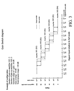
- Multiple gain stages: Implementing multiple gain stages in photodiode circuits can significantly improve dynamic range. This technique involves using different amplification levels for different light intensity ranges, allowing the circuit to adapt to varying light conditions. By combining the outputs from these stages, a wider overall dynamic range can be achieved.
- Time-based integration and reset: Time-based integration and reset mechanisms are employed to extend the dynamic range of photodiode circuits. This approach involves adjusting the integration time or resetting the photodiode at different intervals based on the incoming light intensity. By dynamically controlling these parameters, the circuit can adapt to a broader range of light conditions.
- Dual or multiple photodiode configurations: Using dual or multiple photodiode configurations can enhance the dynamic range of the overall circuit. This technique involves combining photodiodes with different sensitivities or sizes, allowing the circuit to capture a wider range of light intensities. The outputs from these photodiodes are then processed to produce a single, high dynamic range output.
- Adaptive biasing and feedback control: Implementing adaptive biasing and feedback control mechanisms in photodiode circuits can improve dynamic range. These techniques involve dynamically adjusting the bias voltage or current of the photodiode based on the incoming light intensity. Feedback loops are used to optimize the circuit's performance across a wide range of light conditions, ensuring maximum sensitivity and linearity.
02 Multiple gain stages
Implementing multiple gain stages in photodiode circuits can significantly improve dynamic range. This technique involves using different amplification levels for different light intensity ranges, allowing the circuit to adapt to varying light conditions. By combining the outputs from these stages, a wider overall dynamic range can be achieved.Expand Specific Solutions03 Time-based integration and readout
Time-based integration and readout methods can enhance the dynamic range of photodiode circuits. These techniques involve adjusting the integration time or using multiple integration periods to capture both high and low light levels effectively. This approach allows for better handling of scenes with high contrast ratios.Expand Specific Solutions04 Adaptive biasing and reset mechanisms
Adaptive biasing and reset mechanisms are employed to optimize the performance of photodiode circuits across different light conditions. These techniques involve dynamically adjusting the bias voltage or reset timing based on the incoming light intensity, allowing the circuit to maintain sensitivity while avoiding saturation in high-light scenarios.Expand Specific Solutions05 Dual or multi-mode operation
Implementing dual or multi-mode operation in photodiode circuits can extend their dynamic range. This approach involves switching between different operating modes, such as linear and logarithmic, or using multiple photodiodes with different sensitivities. By combining the outputs from these modes or sensors, a wider overall dynamic range can be achieved.Expand Specific Solutions
Key Players in Photodiode and Sensor Industry
The dynamic range optimization in photodiode circuits market is in a growth phase, driven by increasing demand for high-performance imaging solutions across various industries. The market size is expanding, with applications in consumer electronics, automotive, and medical imaging sectors. Technologically, the field is advancing rapidly, with companies like OmniVision Technologies, PixArt Imaging, and Toshiba Corp. leading innovation. These firms are developing sophisticated sensor technologies and integrated circuits to enhance photodiode performance. Research institutions such as California Institute of Technology and Tohoku University are contributing to fundamental advancements, while established players like IBM and Canon are leveraging their extensive R&D capabilities to push the boundaries of dynamic range optimization techniques.
OmniVision Technologies, Inc.
Technical Solution: OmniVision Technologies has developed advanced dynamic range optimization techniques for photodiode circuits in CMOS image sensors. Their approach includes implementing high dynamic range (HDR) technology, which combines multiple exposures to capture both bright and dark areas in a single frame. They utilize a split-diode pixel architecture that allows for dual conversion gain, enabling better performance in low-light conditions while maintaining high dynamic range[1]. OmniVision has also introduced advanced noise reduction algorithms and on-chip image signal processors to further enhance image quality across various lighting conditions[2].
Strengths: Expertise in CMOS image sensors, advanced HDR technology, and integrated image processing. Weaknesses: Potential complexity in implementation and higher cost compared to simpler solutions.
Melexis Technologies NV
Technical Solution: Melexis Technologies has focused on developing innovative solutions for dynamic range optimization in photodiode circuits, particularly for automotive and industrial applications. Their approach includes the use of time-of-flight (ToF) technology combined with advanced signal processing techniques. Melexis has implemented a multi-tap pixel structure that allows for simultaneous capture of different exposure times, significantly expanding the dynamic range[3]. They have also developed proprietary algorithms for on-chip processing to enhance contrast and reduce noise in challenging lighting conditions. Additionally, Melexis has introduced temperature compensation techniques to ensure consistent performance across varying environmental conditions[4].
Strengths: Specialized in automotive and industrial applications, robust performance in harsh environments. Weaknesses: May be less suitable for consumer electronics or applications requiring extremely high resolution.
Core Innovations in Photodiode Circuit Design
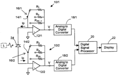
CMOS active pixel sensor with improved dynamic range and method of operation
PatentActiveUS7518645B2
Innovation
- The implementation of a CMOS imaging array with each pixel featuring two distinct amplifier circuits: a lower gain, wide dynamic range amplifier for high light levels and a higher gain, lower dynamic range amplifier for low light levels, allowing for separate output signals to be directed to multiplexers, enabling optimal performance in both conditions.
Measurement system for wide dynamic range optical power meter
PatentInactiveUS7167655B2
Innovation
- A measurement system comprising two current-to-voltage converters with different gains, connected to a photodiode, and a control unit that digitizes and processes signals to selectively switch gains based on predetermined levels, ensuring continuous readings without glitches by overlapping gain settings and introducing hysteresis.
Noise Reduction Strategies in Photodiode Circuits
Noise reduction is a critical aspect of optimizing the dynamic range in photodiode circuits. Various strategies can be employed to minimize noise and enhance the overall performance of these circuits. One of the primary approaches is the implementation of low-noise amplifiers (LNAs) in the front-end of the photodiode circuit. LNAs are designed to amplify weak signals while adding minimal noise, thereby improving the signal-to-noise ratio (SNR) of the system.
Another effective strategy is the use of shielding and proper grounding techniques. Electromagnetic interference (EMI) can significantly contribute to noise in photodiode circuits. By employing proper shielding methods, such as using Faraday cages or conductive enclosures, external electromagnetic noise can be greatly reduced. Additionally, implementing a star-grounding scheme can help minimize ground loops and reduce noise coupling between different circuit components.
Filtering techniques play a crucial role in noise reduction. Low-pass filters can be employed to attenuate high-frequency noise components, while band-pass filters can be used to isolate the desired signal frequency range. In some cases, notch filters may be necessary to eliminate specific noise frequencies, such as those from power line interference.
Temperature stabilization is another important consideration in noise reduction. Thermal noise, also known as Johnson-Nyquist noise, is inherent in all electronic components and increases with temperature. By implementing temperature control mechanisms or choosing components with low temperature coefficients, the impact of thermal noise can be minimized.
Chopper stabilization is an advanced technique that can significantly reduce low-frequency noise, such as 1/f noise, in photodiode circuits. This method involves modulating the input signal to a higher frequency, amplifying it, and then demodulating it back to the original frequency. This process effectively shifts the low-frequency noise to higher frequencies, where it can be more easily filtered out.
Careful component selection and circuit layout design are also crucial for noise reduction. Using low-noise components, such as precision resistors and capacitors, can help minimize intrinsic noise sources. Additionally, optimizing the circuit layout to minimize parasitic capacitances and inductances can reduce noise coupling and improve overall circuit performance.
In digital systems, oversampling and digital filtering techniques can be employed to further reduce noise. By sampling the signal at a much higher rate than the Nyquist frequency and applying digital filtering algorithms, the effective noise floor can be lowered, resulting in improved dynamic range and signal quality.
Applications and Use Cases for Optimized Photodiode Circuits
Optimized photodiode circuits with enhanced dynamic range find applications across various industries and use cases. In the field of medical imaging, these circuits enable more precise diagnostic tools, such as improved X-ray detectors and advanced optical coherence tomography systems. The enhanced sensitivity and wider dynamic range allow for better detection of subtle tissue abnormalities and more accurate disease diagnosis.
In the automotive industry, optimized photodiode circuits play a crucial role in advanced driver assistance systems (ADAS) and autonomous vehicles. They enable more reliable object detection, improved lane departure warning systems, and enhanced adaptive cruise control. The ability to handle a wide range of light intensities is particularly valuable for navigating diverse driving conditions, from bright sunlight to dimly lit tunnels.
Environmental monitoring and atmospheric research benefit greatly from these optimized circuits. They allow for more accurate measurements of air quality, particulate matter, and greenhouse gases. Satellite-based remote sensing systems utilize these circuits to capture high-quality images of Earth's surface, aiding in climate change studies, agricultural monitoring, and natural disaster response.
In the realm of scientific instrumentation, optimized photodiode circuits enhance the capabilities of spectrophotometers, fluorescence microscopes, and other analytical tools. This leads to more sensitive chemical analysis, improved detection of trace elements, and advancements in fields such as materials science and nanotechnology.
The telecommunications industry leverages these circuits in fiber-optic communication systems. They enable faster data transmission rates, longer transmission distances, and improved signal quality in optical networks. This is particularly important for high-speed internet infrastructure and long-distance communication links.
In consumer electronics, optimized photodiode circuits contribute to better performance in devices such as digital cameras, smartphones, and tablets. They enable improved low-light photography, more accurate ambient light sensing for automatic screen brightness adjustment, and enhanced facial recognition capabilities.
Industrial automation and quality control processes benefit from the increased precision offered by these circuits. They enable more accurate optical inspection systems for manufacturing, improved barcode scanners for inventory management, and enhanced machine vision systems for robotic guidance and control.
Unlock deeper insights with PatSnap Eureka Quick Research — get a full tech report to explore trends and direct your research. Try now!
Generate Your Research Report Instantly with AI Agent
Supercharge your innovation with PatSnap Eureka AI Agent Platform!