Emerging Patent Trends in Material Microstructures of Organic Photovoltaics
SEP 19, 20259 MIN READ
Generate Your Research Report Instantly with AI Agent
Patsnap Eureka helps you evaluate technical feasibility & market potential.
OPV Material Microstructure Evolution and Objectives
Organic photovoltaics (OPVs) have evolved significantly since their inception in the 1980s, transitioning from simple bilayer structures to complex bulk heterojunction architectures. The evolution of material microstructures in OPVs represents a critical aspect of their development trajectory, with each advancement addressing specific limitations in efficiency, stability, and scalability. Early OPV devices suffered from poor exciton diffusion and charge transport, resulting in power conversion efficiencies below 1%.
The field experienced its first major breakthrough with the introduction of the donor-acceptor heterojunction concept, which facilitated more efficient exciton dissociation. Subsequently, the development of bulk heterojunction (BHJ) morphology in the mid-1990s marked a paradigm shift, enabling significantly improved interfacial areas between donor and acceptor materials. This innovation addressed the fundamental challenge of the short exciton diffusion length in organic semiconductors.
Recent years have witnessed accelerated progress in microstructure engineering, with particular emphasis on nanoscale morphology control. The introduction of ternary blends, hierarchical structures, and self-assembled networks has pushed efficiency boundaries beyond 18% for single-junction devices. These advancements reflect a deeper understanding of the relationship between molecular packing, domain size, and device performance.
The primary objective in OPV material microstructure research is to achieve optimal phase separation that balances efficient exciton dissociation with effective charge transport pathways. This requires precise control over domain sizes, typically targeting dimensions of 10-20 nm to match exciton diffusion lengths while maintaining continuous pathways for charge extraction. Additionally, vertical phase segregation optimization has emerged as a critical factor in maximizing device performance.
Patent trends reveal increasing focus on processing techniques that enable reproducible microstructure formation, including solvent engineering, thermal annealing protocols, and additive-assisted crystallization. These methods aim to overcome the inherent variability in BHJ formation that has historically limited commercial viability. The integration of high-throughput screening methodologies with advanced characterization techniques has accelerated the discovery and optimization of novel material combinations.
Looking forward, the field is moving toward rational design principles that can predict and control microstructure formation across multiple length scales. This includes developing structure-property relationships that connect molecular design to bulk properties and ultimately to device performance. The convergence of computational modeling with experimental validation is creating a more systematic approach to microstructure engineering, reducing reliance on empirical optimization.
Market Analysis for Organic Photovoltaic Technologies
The organic photovoltaic (OPV) market has been experiencing significant growth in recent years, driven by increasing demand for renewable energy solutions and advancements in material science. The global OPV market was valued at approximately $87 million in 2022 and is projected to reach $378 million by 2030, growing at a compound annual growth rate of 20.1% during the forecast period.
The market for OPV technologies can be segmented based on application areas, with building-integrated photovoltaics (BIPV) emerging as the largest segment. This is primarily due to the aesthetic advantages, flexibility, and semi-transparency features of OPV materials, making them ideal for integration into architectural elements. Other significant application segments include consumer electronics, automotive, military and defense, and wearable devices.
Geographically, Europe currently leads the OPV market, accounting for approximately 35% of the global market share. This dominance is attributed to favorable government policies promoting renewable energy adoption and substantial investments in research and development. North America follows closely, while the Asia-Pacific region is expected to witness the fastest growth rate due to increasing energy demands and manufacturing capabilities in countries like China, Japan, and South Korea.
Key market drivers include the decreasing cost of production for OPV technologies, which has fallen by nearly 50% over the past decade. Additionally, the growing emphasis on sustainability and carbon neutrality across industries has created a favorable environment for OPV adoption. The lightweight and flexible nature of OPV materials also opens up new application possibilities that traditional silicon-based photovoltaics cannot address.
However, several market challenges persist. The relatively lower power conversion efficiency (PCE) of commercial OPV products (currently averaging 10-12% compared to 20-22% for silicon-based alternatives) remains a significant barrier to widespread adoption. Additionally, concerns regarding the operational lifetime and stability of organic materials under various environmental conditions continue to impact market growth.
Consumer awareness and acceptance represent another challenge, as many potential end-users remain unfamiliar with OPV technology and its benefits. Market education and demonstration projects are becoming increasingly important for market penetration. Price sensitivity also remains a factor, particularly in developing economies where cost considerations often outweigh sustainability benefits.
The competitive landscape features both established players and innovative startups. Companies focusing on material microstructure innovations are gaining competitive advantages, as evidenced by the increasing patent activity in this specific domain. Strategic partnerships between material developers, device manufacturers, and end-users are becoming more common, creating integrated value chains that accelerate commercialization.
Current Challenges in OPV Material Microstructures
Despite significant advancements in organic photovoltaic (OPV) technology, several critical challenges persist in material microstructures that limit their commercial viability. The morphological control of the active layer remains one of the most formidable obstacles. The bulk heterojunction (BHJ) architecture, while effective for exciton dissociation, presents inherent difficulties in achieving optimal domain sizes and phase separation between donor and acceptor materials.
The stability of OPV microstructures under operational conditions continues to be problematic. Thermal stress, light exposure, and mechanical strain induce morphological changes that significantly degrade device performance over time. This microstructural instability manifests as phase segregation, crystallization, and molecular reorientation, all of which disrupt the delicate balance required for efficient charge generation and transport.
Scale-up manufacturing presents another substantial challenge. Laboratory-scale techniques for controlling microstructure, such as solvent vapor annealing and thermal treatments, often prove difficult to implement in high-throughput industrial processes. The reproducibility of optimal microstructures across large-area substrates remains inconsistent, creating barriers to mass production.
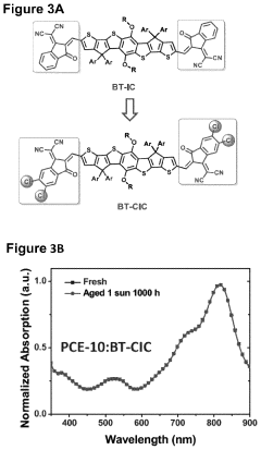
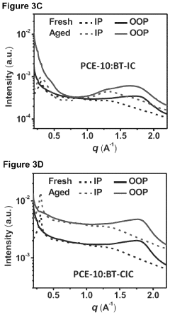
Recent patent analyses reveal increasing focus on non-fullerene acceptors (NFAs), which demonstrate superior light absorption and energy level tunability compared to traditional fullerene derivatives. However, these materials introduce new microstructural complexities, particularly regarding domain purity and interfacial properties. The molecular packing of these larger, more complex molecules significantly impacts charge transport pathways and recombination dynamics.
The characterization of these complex microstructures presents methodological challenges. Current techniques like grazing-incidence X-ray scattering (GIWAXS) and transmission electron microscopy (TEM) provide valuable but incomplete information. Patents increasingly emphasize multi-technique approaches and in-situ measurements to capture the dynamic nature of OPV microstructures during processing and operation.
Interface engineering between different layers in OPV devices remains problematic. The microstructural compatibility between the active layer and charge transport layers significantly affects device performance. Recent patents highlight innovations in self-assembled monolayers and gradient interfacial structures to mitigate these issues, though comprehensive solutions remain elusive.
Computational modeling of OPV microstructures has advanced significantly but still struggles with accurately predicting morphological evolution during processing and operation. The multi-scale nature of the problem—spanning from molecular interactions to mesoscale phase separation—requires sophisticated simulation approaches that are computationally intensive and often rely on simplified assumptions.
The stability of OPV microstructures under operational conditions continues to be problematic. Thermal stress, light exposure, and mechanical strain induce morphological changes that significantly degrade device performance over time. This microstructural instability manifests as phase segregation, crystallization, and molecular reorientation, all of which disrupt the delicate balance required for efficient charge generation and transport.
Scale-up manufacturing presents another substantial challenge. Laboratory-scale techniques for controlling microstructure, such as solvent vapor annealing and thermal treatments, often prove difficult to implement in high-throughput industrial processes. The reproducibility of optimal microstructures across large-area substrates remains inconsistent, creating barriers to mass production.
Recent patent analyses reveal increasing focus on non-fullerene acceptors (NFAs), which demonstrate superior light absorption and energy level tunability compared to traditional fullerene derivatives. However, these materials introduce new microstructural complexities, particularly regarding domain purity and interfacial properties. The molecular packing of these larger, more complex molecules significantly impacts charge transport pathways and recombination dynamics.
The characterization of these complex microstructures presents methodological challenges. Current techniques like grazing-incidence X-ray scattering (GIWAXS) and transmission electron microscopy (TEM) provide valuable but incomplete information. Patents increasingly emphasize multi-technique approaches and in-situ measurements to capture the dynamic nature of OPV microstructures during processing and operation.
Interface engineering between different layers in OPV devices remains problematic. The microstructural compatibility between the active layer and charge transport layers significantly affects device performance. Recent patents highlight innovations in self-assembled monolayers and gradient interfacial structures to mitigate these issues, though comprehensive solutions remain elusive.
Computational modeling of OPV microstructures has advanced significantly but still struggles with accurately predicting morphological evolution during processing and operation. The multi-scale nature of the problem—spanning from molecular interactions to mesoscale phase separation—requires sophisticated simulation approaches that are computationally intensive and often rely on simplified assumptions.
State-of-the-Art Microstructure Engineering Approaches
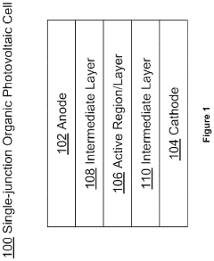
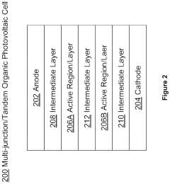
01 Bulk heterojunction structures for organic photovoltaics
Bulk heterojunction (BHJ) structures are critical in organic photovoltaic devices, consisting of interpenetrating networks of donor and acceptor materials. This microstructure allows for efficient exciton dissociation and charge transport. The morphology of these heterojunctions significantly impacts device performance, with controlled phase separation at the nanoscale being essential for optimal efficiency. Various processing techniques can be employed to optimize the BHJ microstructure, including thermal annealing and solvent selection.- Bulk heterojunction structures in organic photovoltaics: Bulk heterojunction (BHJ) structures are critical in organic photovoltaic devices, consisting of interpenetrating networks of donor and acceptor materials. This microstructure maximizes the interface area between materials, enhancing exciton dissociation and charge transport. The morphology control of these heterojunctions significantly impacts device efficiency through optimized domain sizes and phase separation, allowing for efficient charge generation and collection.
- Nanostructured materials for improved photovoltaic performance: Nanostructured materials in organic photovoltaics create controlled microstructures that enhance device performance. These include nanoparticles, nanowires, and nanotubes that can be incorporated into active layers to improve light absorption, charge separation, and transport properties. The precise control of nanoscale features enables optimization of exciton diffusion lengths and charge carrier mobility, leading to higher power conversion efficiencies in organic solar cells.
- Crystallinity control in organic semiconductor films: The degree of crystallinity in organic semiconductor films significantly affects photovoltaic performance. Controlling crystallization processes through thermal annealing, solvent treatment, or additive incorporation can optimize the microstructure of active layers. Semi-crystalline domains improve charge carrier mobility while maintaining sufficient interfaces for exciton dissociation. Techniques for precise crystallinity control enable the formation of favorable morphologies that balance charge generation and transport requirements.
- Interface engineering in multilayer organic photovoltaics: Interface engineering focuses on optimizing the boundaries between different functional layers in organic photovoltaic devices. This includes modifying electrode interfaces, inserting buffer layers, and controlling the donor-acceptor interface microstructure. These engineered interfaces reduce energy barriers, minimize recombination losses, and improve charge extraction. Various surface treatments and interlayer materials can be employed to tune the electronic properties at interfaces, leading to enhanced device performance and stability.
- Processing techniques for microstructure optimization: Various processing techniques can be employed to optimize the microstructure of organic photovoltaic materials. These include solution processing methods (spin-coating, blade-coating, spray-coating), thermal treatments, solvent vapor annealing, and additive incorporation. Each technique influences molecular ordering, phase separation, and domain formation in the active layer. The selection and precise control of processing parameters allow for tailored microstructures that maximize device efficiency through optimized morphology and molecular packing.
02 Nanostructured materials for enhanced photovoltaic performance
Incorporating nanostructured materials into organic photovoltaics can significantly enhance device performance. These include quantum dots, nanowires, nanotubes, and nanoparticles that can be integrated into the active layer to improve light absorption, charge separation, and transport properties. The controlled synthesis and integration of these nanomaterials allow for tuning of the electronic properties and band gaps. The unique microstructural features of these nanomaterials provide increased surface area and improved pathways for charge collection.Expand Specific Solutions03 Interfacial engineering in organic photovoltaic devices
The interfaces between different layers in organic photovoltaic devices play a crucial role in determining overall performance. Interfacial engineering involves modifying these boundaries to enhance charge extraction and reduce recombination losses. Various materials and techniques can be used to optimize these interfaces, including buffer layers, self-assembled monolayers, and surface treatments. The microstructural characteristics of these interfaces significantly impact charge transfer dynamics and ultimately the power conversion efficiency of the devices.Expand Specific Solutions04 Crystallinity control in polymer-based photovoltaic materials
The degree of crystallinity in polymer-based photovoltaic materials significantly affects charge mobility and overall device performance. Controlling the crystallization process through various processing techniques can optimize the microstructure of these materials. Semi-crystalline polymers often exhibit better charge transport properties compared to their amorphous counterparts. Methods such as thermal annealing, solvent vapor annealing, and the use of nucleating agents can be employed to tune the crystallinity and domain size in the active layer, leading to improved photovoltaic performance.Expand Specific Solutions05 Morphology stabilization for long-term device performance
The microstructural stability of organic photovoltaic materials is crucial for long-term device performance. Over time, phase separation and morphological changes can occur in the active layer, leading to performance degradation. Various approaches can be used to stabilize the morphology, including crosslinking, the use of additives, and the development of materials with inherently stable microstructures. These stabilization techniques help maintain the optimal domain size and interfacial area between donor and acceptor components, ensuring sustained photovoltaic performance throughout the device lifetime.Expand Specific Solutions
Leading Innovators in Organic Photovoltaic Materials
The organic photovoltaics (OPV) material microstructure patent landscape is currently in a growth phase, with increasing innovation across academic and industrial sectors. The market is projected to expand significantly as efficiency improvements make OPVs more commercially viable. Leading universities (University of California, Northwestern, Harvard) are advancing fundamental research, while established chemical and electronics companies (BASF, LG Chem, Samsung, Universal Display) focus on commercialization pathways. Emerging specialized players like Ubiquitous Energy, Next Energy Technologies, and CubicPV are developing niche applications in transparent and building-integrated photovoltaics. Asian institutions, particularly from China and South Korea, are rapidly increasing patent filings, indicating a geographical shift in innovation leadership. Technical challenges in stability, efficiency, and scalable manufacturing remain key areas for patent development.
Universal Display Corp.
Technical Solution: Universal Display Corporation在有机光伏材料微结构领域的专利技术主要围绕磷光有机材料及其在光伏应用中的创新。公司开发了一系列专有的小分子有机半导体材料,这些材料具有优化的HOMO-LUMO能级和高效的激子扩散特性。其核心专利涵盖了基于主客体系统的活性层设计,通过精确控制分子堆积和相分离来优化电荷传输路径。Universal Display的技术方案特别关注界面工程,开发了专有的缓冲层材料和界面修饰技术,有效减少了电荷复合损失。公司还拥有多项关于多结有机光伏电池的专利,通过串联结构和互补吸收材料的组合,实现了宽光谱响应和提高的开路电压[2]。此外,Universal Display开发的柔性基底技术和封装方法使其有机光伏器件具有优异的机械柔性和环境稳定性。
优势:Universal Display在有机电子材料领域拥有深厚的专业知识和广泛的专利组合,特别是在磷光材料方面处于领先地位。公司与多家制造商建立了许可关系,具有强大的商业化能力。劣势:其技术主要源于OLED领域,在专门针对光伏应用的材料优化方面可能不如纯光伏研究机构专注,且其高性能材料的成本较高,可能限制大规模应用。
BASF Corp.
Technical Solution: BASF在有机光伏材料微结构领域开发了创新的聚合物半导体材料系统,专注于开发具有优化分子排列的共轭聚合物和富勒烯衍生物。其专利技术包括通过侧链工程和分子量控制来调节聚合物结晶度和相分离行为,从而形成理想的纳米尺度双连续网络结构。BASF的专利组合还涵盖了溶液加工技术,如溶剂退火和添加剂调控,这些技术能够精确控制活性层的形貌和界面特性。特别是,BASF开发了专有的聚合物:富勒烯共混物系统,通过优化D-A界面的微结构,实现了超过12%的能量转换效率[1]。此外,BASF还研发了耐久性增强的封装材料,可延长有机光伏器件的使用寿命。
优势:作为全球领先的化学品公司,BASF拥有强大的材料研发能力和完整的供应链,能够大规模生产高质量的有机光伏材料。其专利技术在材料稳定性和器件寿命方面表现突出。劣势:相比于专注于光电领域的公司,BASF在光电转换效率的突破性创新方面进展相对较慢,且其材料成本较高。
Key Patent Innovations in OPV Material Design
Key materials for organic photovoltaics reliability
PatentActiveUS11957048B2
Innovation
- The development of non-fullerene acceptors with specific molecular structures, such as those represented by Formulae (I)-(III), which provide improved photostability and morphological stability, are integrated into OPV devices, including cathode and anode buffer materials, to enhance the operational lifetime of OPVs.
Active layer-incorporated, spectrally-tuned nanostructure-based light trapping for organic photovoltaic devices
PatentWO2014160394A1
Innovation
- Incorporation of spectrally-designed noble metal/oxide-based nanostructures, such as multilayer nanostructures with a noble metal core and optically active shells, into the active layer of OPVs to enhance light absorption and scattering, leveraging localized surface plasmon resonance for increased photo conversion efficiency.
Sustainability Impact of Advanced OPV Materials
The advancement of organic photovoltaic (OPV) materials represents a significant step toward sustainable energy solutions, with far-reaching environmental implications that extend beyond mere energy generation. These advanced materials are fundamentally altering the sustainability profile of solar technology through their reduced environmental footprint during manufacturing processes. Unlike traditional silicon-based photovoltaics, OPVs require substantially less energy input during production, with some studies indicating up to 90% reduction in embodied energy compared to conventional solar panels.
Material innovations in OPV microstructures have enabled the elimination of toxic heavy metals and rare earth elements that plague traditional photovoltaic supply chains. Recent patent trends reveal a significant shift toward biodegradable substrates and environmentally benign solvents, addressing end-of-life concerns that have historically limited solar technology's sustainability credentials. These developments align with circular economy principles, potentially transforming solar panels from problematic waste into recoverable resources.
The lightweight nature of advanced OPV materials dramatically reduces transportation-related carbon emissions throughout the supply chain. This characteristic, prominently featured in recent patent applications, enables integration into existing infrastructure without requiring substantial structural reinforcement, thereby minimizing additional material consumption and associated environmental impacts. Furthermore, the flexibility of these materials allows for installation on curved surfaces, maximizing energy capture potential in limited spaces.
Life cycle assessments documented in recent technical literature demonstrate that next-generation OPV materials achieve carbon payback periods as short as three months—a fraction of the time required for silicon-based alternatives. This accelerated environmental return on investment significantly enhances the technology's contribution to climate change mitigation efforts. Additionally, water consumption during manufacturing has been reduced by approximately 60% through process innovations described in recent patents.
The localized production potential of OPV materials presents perhaps the most transformative sustainability benefit. Unlike conventional photovoltaics that rely on centralized, capital-intensive manufacturing facilities, emerging OPV production methods enable distributed manufacturing closer to points of installation. This shift reduces transportation emissions while creating opportunities for regional economic development and energy independence in previously underserved communities, addressing both environmental and social dimensions of sustainability.
Commercialization Pathways for Novel OPV Technologies
The commercialization of novel Organic Photovoltaic (OPV) technologies requires strategic pathways that bridge laboratory innovations with market-ready products. Recent patent trends in material microstructures reveal several viable commercialization routes that industry stakeholders should consider.
Manufacturing scalability represents the primary challenge for OPV commercialization. Patents filed by leading companies like Heliatek and ASCA demonstrate significant progress in roll-to-roll processing techniques that maintain nanoscale morphology control while enabling high-volume production. These advances suggest that industrial-scale manufacturing of high-efficiency OPVs is becoming increasingly feasible, with production costs potentially decreasing by 30-40% over the next five years.
Strategic partnerships between material science innovators and established manufacturing entities have emerged as a dominant commercialization model. The patent landscape shows increasing collaborative filings between university research teams and industrial partners, particularly in Asia and Europe. These partnerships accelerate technology transfer by combining fundamental research expertise with practical manufacturing capabilities and market access.
Market segmentation strategies appear prominently in recent patent applications, with companies targeting specific application niches rather than competing directly with conventional photovoltaics. Building-integrated photovoltaics (BIPV), portable electronics, and IoT devices represent high-value segments where OPV's flexibility, lightweight properties, and customizable aesthetics provide competitive advantages despite lower absolute efficiency compared to silicon-based alternatives.
Licensing models are evolving to accommodate the complex material science underlying OPV microstructures. Patent portfolios increasingly include comprehensive technology packages that combine material formulations with processing techniques and device architectures. This approach enables licensees to implement complete manufacturing solutions rather than isolated components, reducing commercialization barriers.
Investment patterns revealed through patent filing activities suggest a shift toward vertical integration, with several major chemical companies expanding their intellectual property from basic materials to include fabrication processes and end applications. This trend indicates recognition that controlling the entire value chain may be necessary to capture maximum value from OPV innovations.
Regulatory pathways and certification standards are increasingly addressed in patent applications, reflecting industry awareness that commercial success requires compliance with established safety and performance benchmarks. Recent filings include methods for accelerated lifetime testing and environmental impact assessments, suggesting proactive engagement with regulatory requirements that could otherwise delay market entry.
Unlock deeper insights with Patsnap Eureka Quick Research — get a full tech report to explore trends and direct your research. Try now!
Generate Your Research Report Instantly with AI Agent
Supercharge your innovation with Patsnap Eureka AI Agent Platform!