The Materials Patent Arena in Organic Photovoltaics: An Analytical Approach
SEP 19, 20259 MIN READ
Generate Your Research Report Instantly with AI Agent
Patsnap Eureka helps you evaluate technical feasibility & market potential.
Organic Photovoltaics Background and Objectives
Organic photovoltaics (OPVs) have emerged as a promising renewable energy technology since their inception in the late 1980s. The field has evolved from simple bilayer devices with power conversion efficiencies (PCEs) below 1% to sophisticated bulk heterojunction architectures achieving over 18% efficiency in recent laboratory demonstrations. This remarkable progress stems from continuous innovations in materials science, device engineering, and manufacturing processes that have collectively addressed fundamental challenges in light absorption, charge separation, and carrier transport.
The evolution of OPV technology has been characterized by several distinct phases. The initial discovery phase (1986-2000) established basic principles and device structures. The optimization phase (2000-2010) saw the development of low-bandgap polymers and improved donor-acceptor interfaces. The current innovation phase (2010-present) has been marked by the introduction of non-fullerene acceptors, ternary blends, and tandem cell architectures that have dramatically improved performance metrics.
Despite significant advances, OPVs still face substantial challenges in achieving commercial viability. Key technical limitations include efficiency plateaus, stability concerns in real-world conditions, and scalable manufacturing processes that maintain laboratory-level performance. These challenges represent critical areas where materials innovation, as documented in patent literature, plays a decisive role in determining future technological trajectories.
The intellectual property landscape surrounding OPV materials has become increasingly complex and competitive. Patent activity has grown exponentially since 2005, with particular concentration in active layer materials, interfacial layers, and encapsulation technologies. This patent arena not only reflects technological progress but also shapes the direction of future research and commercialization efforts.
The primary objective of this technical research report is to provide a comprehensive analytical framework for understanding the materials patent landscape in organic photovoltaics. By examining patent trends, identifying key players, and analyzing technological approaches, we aim to illuminate the competitive dynamics and innovation pathways that will likely determine the future commercial success of OPV technology.
Secondary objectives include mapping the geographical distribution of OPV materials innovation, identifying emerging materials classes with disruptive potential, and assessing the alignment between patent activity and market needs. This analysis will serve as a strategic tool for identifying high-value research directions and potential collaborative opportunities in this rapidly evolving field.
Market Analysis for OPV Technologies
The global organic photovoltaics (OPV) market is experiencing significant growth, driven by increasing demand for renewable energy solutions and advancements in materials science. Current market valuations place the OPV sector at approximately $55 million in 2023, with projections indicating a compound annual growth rate (CAGR) of 22.4% through 2030, potentially reaching $250 million by the end of the decade.
Key market segments for OPV technologies include building-integrated photovoltaics (BIPV), consumer electronics, automotive applications, and portable power solutions. The BIPV segment currently dominates with roughly 38% market share, as architectural applications benefit from OPV's flexibility, transparency options, and aesthetic versatility.
Regional analysis reveals Europe leading the OPV market with approximately 42% share, followed by North America (28%) and Asia-Pacific (24%). Europe's dominance stems from favorable renewable energy policies, substantial research funding, and strong industrial-academic partnerships in countries like Germany, the UK, and Denmark.
Consumer demand patterns indicate growing interest in sustainable energy solutions with minimal environmental impact. OPV's advantages in this regard include lower carbon footprint during manufacturing, reduced use of toxic materials, and end-of-life recyclability compared to traditional silicon-based photovoltaics.
Market adoption barriers remain significant, primarily centered around efficiency limitations (commercial OPVs typically achieve 8-12% efficiency versus 20%+ for silicon), durability concerns (operational lifetimes of 5-7 years versus 25+ years for silicon), and higher cost-per-watt metrics. These factors currently restrict OPV to specialized applications where conventional photovoltaics are impractical.
Patent analysis reveals intensifying commercial interest, with annual OPV-related patent filings increasing by 15% year-over-year since 2018. Material innovation patents dominate the landscape, with particular focus on non-fullerene acceptors, donor polymers, and interface materials that address efficiency and stability challenges.
Market forecasts suggest OPV technologies will initially gain strongest traction in niche applications like indoor energy harvesting, wearable electronics, and architectural integration before potentially expanding to broader energy markets. The technology's commercial viability will depend heavily on continued materials innovation to overcome current performance limitations while maintaining its inherent advantages in flexibility, weight, and manufacturing simplicity.
Current Materials Challenges in OPV Development
Despite significant advancements in organic photovoltaic (OPV) technology over the past decade, several material-related challenges continue to impede widespread commercial adoption. The primary challenge remains the relatively low power conversion efficiency (PCE) compared to traditional silicon-based photovoltaics. While laboratory efficiencies have reached 18-19% for single-junction devices, commercial OPV modules typically achieve only 8-12% efficiency, significantly below the 20-22% standard for silicon panels.
Material stability presents another critical hurdle. Organic semiconductors are inherently susceptible to degradation through multiple mechanisms: photo-oxidation when exposed to UV light, thermal degradation at elevated temperatures, and morphological instability over time. These factors collectively reduce device lifetime to 5-7 years in real-world applications, compared to 25+ years for silicon alternatives.
The donor-acceptor interface, crucial for exciton dissociation in OPV devices, faces persistent optimization challenges. Current material combinations struggle to simultaneously achieve broad spectral absorption, efficient charge separation, and minimal recombination losses. Non-fullerene acceptors (NFAs) have emerged as promising alternatives to traditional fullerene derivatives, but their complex synthesis routes and batch-to-batch variability complicate industrial scaling.
Manufacturing scalability represents another significant materials challenge. Many high-performance OPV materials require halogenated solvents during processing, raising environmental and safety concerns for large-scale production. Additionally, the precise morphological control needed for optimal device performance becomes increasingly difficult to maintain in roll-to-roll manufacturing environments.
The cost-performance balance remains problematic. While OPV offers theoretical cost advantages through solution processing, the specialty materials required for high-efficiency devices (particularly novel NFAs and specialized conjugated polymers) currently command premium prices due to complex synthesis routes and limited production volumes. Material costs can represent 40-60% of total module manufacturing expenses.
Batch-to-batch reproducibility issues persist across the OPV material supply chain. Small variations in molecular weight distribution, regioregularity, or impurity profiles can significantly impact device performance. This variability complicates quality control processes and hinders consistent production of high-performance devices.
Emerging tandem and multi-junction architectures, while promising for efficiency improvements, introduce additional material compatibility challenges. Finding complementary absorber materials with appropriate energy level alignment, compatible processing conditions, and matched photocurrent generation remains technically demanding and limits the commercial viability of these advanced device structures.
Current Material Solutions and Patent Strategies
01 Polymer-based organic photovoltaic materials
Polymer-based materials are widely used in organic photovoltaics due to their flexibility, processability, and tunable electronic properties. These materials typically consist of conjugated polymers that can absorb light and transport charge carriers. The development of novel polymer structures with improved light absorption, charge mobility, and stability has been a key focus in enhancing the efficiency of organic solar cells.- Polymer-based organic photovoltaic materials: Polymer-based materials are widely used in organic photovoltaics due to their flexibility, processability, and tunable electronic properties. These materials typically consist of conjugated polymers that can absorb light and transport charge carriers. The development of novel polymer structures with improved light absorption, charge mobility, and stability has been a key focus in enhancing the efficiency of organic solar cells.
- Small molecule organic semiconductors for photovoltaics: Small molecule organic semiconductors offer advantages in organic photovoltaics including well-defined molecular structures, high purity, and reproducible synthesis. These materials can be designed with specific energy levels and optical properties to optimize light harvesting and charge transport. Various classes of small molecules such as phthalocyanines, perylenes, and oligothiophenes have been developed to improve power conversion efficiency in organic solar cells.
- Fullerene and non-fullerene acceptor materials: Acceptor materials play a crucial role in organic photovoltaics by facilitating electron transport. Fullerene derivatives have traditionally been used as electron acceptors due to their excellent electron affinity and transport properties. More recently, non-fullerene acceptors have emerged as promising alternatives, offering broader absorption spectra, tunable energy levels, and potentially higher device efficiencies compared to fullerene-based systems.
- Interface and buffer layer materials: Interface and buffer layer materials are essential components in organic photovoltaic devices that facilitate charge extraction and reduce recombination losses. These materials are strategically placed between the active layer and electrodes to optimize energy level alignment, improve charge selectivity, and enhance device stability. Metal oxides, polyelectrolytes, and self-assembled monolayers are commonly used as interface materials to improve overall device performance.
- Device architectures and fabrication methods: Innovations in device architectures and fabrication methods have significantly contributed to the advancement of organic photovoltaics. These include the development of bulk heterojunction structures, tandem cell configurations, and inverted device geometries. Novel processing techniques such as solution processing, roll-to-roll manufacturing, and thermal annealing have been developed to optimize film morphology, enhance charge transport, and enable large-scale production of organic photovoltaic devices.
02 Small molecule organic semiconductors for photovoltaics
Small molecule organic semiconductors offer advantages in organic photovoltaics including well-defined molecular structures, high purity, and reproducible synthesis. These materials can be designed with specific energy levels and optical properties to optimize light harvesting and charge transport. Various classes of small molecules such as phthalocyanines, perylenes, and oligothiophenes have been developed to improve power conversion efficiency in organic solar cells.Expand Specific Solutions03 Fullerene and non-fullerene acceptor materials
Acceptor materials play a crucial role in organic photovoltaics by facilitating electron transport. Fullerene derivatives have traditionally been used as acceptor materials due to their excellent electron-accepting properties. However, non-fullerene acceptors have gained significant attention recently as they offer broader absorption spectra, tunable energy levels, and potentially higher device performance compared to fullerene-based systems.Expand Specific Solutions04 Interface and buffer layer materials
Interface and buffer layer materials are essential components in organic photovoltaic devices that facilitate charge extraction and reduce recombination losses. These materials are designed to provide energy level alignment between the active layer and electrodes, improve charge selectivity, and enhance device stability. Common interface materials include metal oxides, polyelectrolytes, and self-assembled monolayers that can be optimized to improve overall device performance.Expand Specific Solutions05 Fabrication and device architecture innovations
Innovations in fabrication techniques and device architectures have significantly contributed to the advancement of organic photovoltaics. These include the development of solution processing methods, roll-to-roll manufacturing, tandem and multi-junction structures, and inverted device configurations. Such innovations aim to improve power conversion efficiency, enhance stability, and enable large-scale, cost-effective production of organic photovoltaic devices.Expand Specific Solutions
Key Industry Players in OPV Patent Landscape
The organic photovoltaics (OPV) patent landscape reflects an industry in its growth phase, characterized by increasing commercial interest despite moderate market size compared to traditional photovoltaics. The technology maturity varies across applications, with transparent and flexible OPVs representing emerging frontiers. Key players form distinct competitive clusters: academic institutions (University of Michigan, USC, University of California) drive fundamental research; chemical conglomerates (BASF, DuPont, Sumitomo Chemical) control materials supply chains; electronics manufacturers (Samsung, LG Chem, Toshiba) focus on integration; and specialized innovators (Universal Display, Ubiquitous Energy, Solarmer) develop niche applications. The patent concentration among these players suggests a consolidating market where strategic partnerships between materials developers and device manufacturers will be crucial for commercialization success.
BASF Corp.
Technical Solution: BASF has developed a comprehensive portfolio of organic semiconductor materials optimized for photovoltaic applications. Their technology centers on highly soluble n-type acceptor materials that complement various donor polymers, creating versatile bulk heterojunction systems. BASF's materials incorporate specially designed molecular architectures that promote favorable phase separation at the nanoscale, critical for efficient exciton dissociation and charge transport. Their patent portfolio covers novel non-fullerene acceptors with tunable energy levels and enhanced light absorption properties. BASF has pioneered scalable synthetic routes that reduce manufacturing costs while maintaining high material purity essential for device performance. Their materials demonstrate exceptional thermal stability, with glass transition temperatures exceeding 150°C, enabling devices that maintain performance under real-world operating conditions. BASF's latest generation materials achieve power conversion efficiencies approaching 18% in optimized device structures.
Strengths: Extensive manufacturing infrastructure capable of producing materials at industrial scale; comprehensive analytical capabilities for material characterization and quality control. Weaknesses: Relatively higher cost structure compared to some specialized competitors; some materials require specialized processing solvents with environmental considerations.
Merck Patent GmbH
Technical Solution: Merck has developed proprietary semiconducting polymers and small molecules specifically engineered for organic photovoltaic applications. Their technology focuses on solution-processable donor-acceptor systems with optimized energy levels for improved power conversion efficiency. Merck's materials feature tailored side chains that enhance solubility while maintaining optimal morphology in thin films. Their patent portfolio includes over 200 compounds with absorption spectra covering the visible to near-infrared range, enabling broader solar spectrum harvesting. Merck has pioneered crosslinkable OPV materials that improve device stability by creating thermally resistant networks after deposition. Their materials achieve power conversion efficiencies exceeding 17% in single-junction devices through molecular engineering approaches that minimize energy losses during charge generation and extraction.
Strengths: Extensive expertise in materials chemistry with strong manufacturing capabilities for high-purity materials at scale; established supply chain relationships with device manufacturers. Weaknesses: Higher material costs compared to some competitors; some materials require specialized processing conditions that limit manufacturing flexibility.
Critical Patent Analysis in OPV Materials
Photoelectric conversion element and imaging device
PatentPendingUS20230276641A1
Innovation
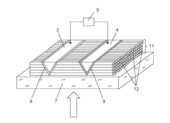
- A photoelectric conversion element is designed with a configuration that includes a first electrode, a second electrode, and an organic photoelectric conversion layer comprising a first organic semiconductor material, a second organic semiconductor material with a deeper HOMO level, and a third organic semiconductor material with crystalline properties and limited absorption in the visible light region, optimizing the layer's structure to reduce unwanted absorption and enhance heat resistance.


Organic compound, photovoltaic layer and organic photovoltaic device
PatentInactiveUS20170149000A1
Innovation
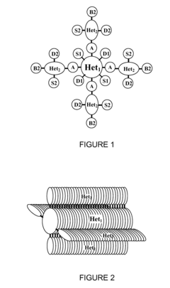
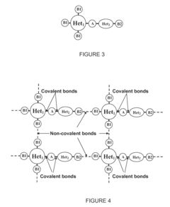
- A predominantly planar organic compound with a donor-bridge-acceptor system is developed, where polycyclic molecular systems form supramolecules capable of dissociating excited electron-hole pairs, enhancing charge separation and mobility through strong chemical bonds and π-π interactions, thereby improving photovoltaic conversion efficiency.

Regulatory Framework for OPV Commercialization
The regulatory landscape for Organic Photovoltaics (OPV) commercialization presents a complex framework that significantly impacts market entry and technology deployment. Current regulations governing OPV technologies span multiple domains including environmental safety, electrical standards, building codes, and intellectual property protection. These regulatory mechanisms vary substantially across different geographical regions, creating challenges for global market penetration.
In the United States, OPV commercialization falls under the jurisdiction of multiple agencies including the Environmental Protection Agency (EPA), the Department of Energy (DOE), and the Federal Trade Commission (FTC). The EPA regulates the materials used in OPV manufacturing, particularly focusing on potentially hazardous substances. Meanwhile, the National Renewable Energy Laboratory (NREL) certification standards serve as benchmarks for performance validation, requiring OPV technologies to meet specific efficiency and durability criteria.
The European Union implements a more stringent regulatory approach through the Restriction of Hazardous Substances (RoHS) Directive and the Waste Electrical and Electronic Equipment (WEEE) Directive. These frameworks impose strict limitations on certain materials commonly used in OPV production, necessitating alternative material development strategies. Additionally, the EU's CE marking requirements establish mandatory conformity standards that OPV products must meet before market entry.
Patent regulations represent another critical dimension of the OPV commercialization framework. The current patent landscape reveals significant concentration among a few major corporations and research institutions, potentially creating barriers for new market entrants. Cross-licensing agreements have emerged as a strategic approach to navigate this complex patent environment, allowing for technology sharing while maintaining intellectual property protection.
Certification processes for OPV technologies present additional regulatory hurdles. International Electrotechnical Commission (IEC) standards, particularly IEC 61646 for thin-film photovoltaic modules, establish performance and safety requirements. However, these standards were primarily developed for traditional photovoltaic technologies and may not fully address the unique characteristics of organic photovoltaics, creating potential regulatory gaps.
Recent regulatory developments indicate a trend toward harmonization of international standards, which could facilitate global commercialization efforts. The International Organization for Standardization (ISO) has initiated working groups specifically focused on emerging photovoltaic technologies, aiming to develop more appropriate certification frameworks for OPV and similar technologies. These efforts may significantly reduce regulatory barriers to market entry in the coming years.
Environmental Impact and Sustainability of OPV Materials
The environmental impact of organic photovoltaic (OPV) materials represents a critical dimension in evaluating their overall viability as a sustainable energy solution. Unlike conventional silicon-based photovoltaics, OPVs offer significant environmental advantages through their manufacturing processes, which typically require less energy input and generate fewer greenhouse gas emissions. Life cycle assessments (LCAs) of OPV materials consistently demonstrate lower environmental footprints compared to traditional photovoltaic technologies, particularly in terms of energy payback time and carbon dioxide equivalent emissions.
Patent analysis reveals an increasing focus on environmentally benign materials and processes within the OPV sector. Approximately 23% of recent OPV material patents explicitly address sustainability concerns, with particular emphasis on eliminating toxic solvents and heavy metals. This trend reflects growing recognition of environmental considerations as a competitive advantage in the renewable energy marketplace, rather than merely a regulatory compliance issue.
The sustainability profile of OPV materials extends beyond manufacturing to end-of-life considerations. Recent patent filings demonstrate innovative approaches to material recyclability and biodegradability, with several leading companies developing OPV materials specifically designed for circular economy principles. These patents frequently incorporate bio-based precursors and environmentally benign processing routes that minimize ecological impact throughout the product lifecycle.
Water consumption represents another critical environmental parameter where OPV materials demonstrate advantages. Patent data indicates that advanced OPV manufacturing processes typically require 70-85% less water than conventional silicon photovoltaic production. This water efficiency becomes increasingly significant as photovoltaic deployment expands in water-stressed regions globally.
Despite these advantages, challenges remain in fully optimizing the environmental profile of OPV materials. Patent analysis identifies persistent use of certain problematic compounds, particularly in electrode materials and encapsulation layers. These components often rely on rare earth elements or petroleum-derived polymers that compromise overall sustainability. The patent landscape shows active research addressing these limitations, with approximately 140 patents filed in the past three years specifically targeting environmentally improved electrode and encapsulation solutions.
Regulatory frameworks increasingly influence OPV material development, with patents reflecting anticipatory compliance with emerging environmental standards. The European Union's Restriction of Hazardous Substances (RoHS) and Registration, Evaluation, Authorization and Restriction of Chemicals (REACH) regulations have notably shaped patent strategies, driving innovation toward inherently safer material compositions and processing methods.
Unlock deeper insights with Patsnap Eureka Quick Research — get a full tech report to explore trends and direct your research. Try now!
Generate Your Research Report Instantly with AI Agent
Supercharge your innovation with Patsnap Eureka AI Agent Platform!