Mass Transfer Challenges in the Commercial Scale-Up of Organic Photovoltaics
SEP 19, 20259 MIN READ
Generate Your Research Report Instantly with AI Agent
Patsnap Eureka helps you evaluate technical feasibility & market potential.
OPV Scale-Up Background and Objectives
Organic Photovoltaics (OPV) technology has evolved significantly since the discovery of conductive polymers in the 1970s, which earned Alan Heeger, Alan MacDiarmid, and Hideki Shirakawa the Nobel Prize in Chemistry in 2000. The field has progressed from initial power conversion efficiencies (PCEs) below 1% to current laboratory-scale devices exceeding 18% for single-junction cells and approaching 20% for tandem architectures. This remarkable advancement has positioned OPVs as a promising alternative to traditional silicon-based photovoltaics, particularly for applications requiring flexibility, lightweight properties, and semi-transparency.
The technological evolution of OPVs has been characterized by several key breakthroughs, including the development of bulk heterojunction architectures, non-fullerene acceptors, and advanced interfacial materials. These innovations have addressed fundamental limitations in charge generation, transport, and collection, significantly improving device performance and stability. However, the transition from laboratory success to commercial viability remains challenging, with mass transfer phenomena emerging as a critical bottleneck in the scale-up process.
Current market trends indicate growing demand for sustainable energy solutions, with the global photovoltaic market projected to reach $300 billion by 2030. Within this landscape, OPVs offer unique value propositions in building-integrated photovoltaics, portable electronics, and IoT applications. The technology's compatibility with roll-to-roll manufacturing processes presents opportunities for cost-effective large-scale production, potentially reducing the levelized cost of electricity to competitive levels.
The primary objective of this technical research is to comprehensively analyze the mass transfer challenges that emerge during the commercial scale-up of OPV manufacturing. These challenges include solvent evaporation dynamics, layer thickness uniformity, interface formation, and morphological control across large areas. Understanding these phenomena is crucial for translating laboratory efficiencies to commercial-scale production while maintaining performance metrics.
Secondary objectives include identifying scalable manufacturing techniques that can effectively address these mass transfer limitations, evaluating the impact of different processing parameters on device performance at commercial scales, and developing predictive models that can guide process optimization. Additionally, this research aims to establish correlations between processing conditions, mass transfer phenomena, and the resulting device characteristics.
The ultimate goal is to establish a technological roadmap that bridges the gap between laboratory demonstrations and commercial manufacturing, enabling the realization of OPV's full potential in the renewable energy landscape. This requires not only addressing current technical challenges but also anticipating future developments in materials, processing techniques, and application requirements.
Market Analysis for Commercial OPV Technology
The global organic photovoltaics (OPV) market is experiencing significant growth, driven by increasing demand for renewable energy solutions and advancements in flexible electronics. Current market valuations place the OPV sector at approximately $87 million in 2023, with projections indicating a compound annual growth rate (CAGR) of 22.4% through 2030, potentially reaching $380 million by the end of the decade.
Key market segments for OPV technology include building-integrated photovoltaics (BIPV), consumer electronics, automotive applications, and portable power solutions. The BIPV segment currently dominates market share at 42%, leveraging OPV's aesthetic advantages and form factor flexibility. Consumer electronics represents the fastest-growing segment with 28% annual growth, particularly in wearable technology and IoT devices.
Geographically, Europe leads OPV market adoption with 38% market share, followed by North America (29%) and Asia-Pacific (26%). China and South Korea are rapidly expanding their OPV manufacturing capabilities, potentially shifting the market balance within the next five years. Government incentives for renewable energy in the EU and parts of Asia are creating favorable market conditions for OPV commercialization.
Market drivers include decreasing manufacturing costs, which have fallen by 35% over the past three years, and increasing efficiency rates, which have improved from 3-5% to 15-17% in laboratory settings. The lightweight and flexible nature of OPV technology opens niche markets inaccessible to traditional silicon-based photovoltaics.
Consumer demand analysis reveals growing preference for sustainable energy solutions, with 67% of surveyed consumers expressing willingness to pay premium prices for products incorporating green energy technology. Corporate sustainability initiatives are further driving B2B demand, with 78% of Fortune 500 companies having established renewable energy targets.
Market barriers include competition from established photovoltaic technologies, particularly perovskite solar cells which achieved 25.7% efficiency in recent demonstrations. Scale-up challenges specifically related to mass transfer issues during manufacturing represent a significant market entry barrier, increasing production costs by an estimated 30-40% compared to theoretical minimums.
Industry analysts forecast that successful resolution of mass transfer challenges in commercial-scale production could reduce manufacturing costs by 45%, potentially expanding the addressable market by 2.5 times current projections and accelerating market penetration in price-sensitive segments.
Mass Transfer Barriers in Large-Scale OPV Production
Mass transfer challenges represent one of the most significant barriers in scaling up organic photovoltaic (OPV) production from laboratory to commercial levels. At the laboratory scale, solution-based processing techniques like spin coating provide excellent control over film thickness and morphology. However, these methods become impractical when transitioning to large-area manufacturing, creating a fundamental mass transfer bottleneck.
The primary mass transfer challenge involves achieving uniform deposition of active layer materials across large substrate areas. In roll-to-roll (R2R) processing, maintaining consistent solution flow dynamics becomes increasingly difficult as width increases. Edge effects and surface tension variations lead to thickness inconsistencies that dramatically impact device performance and yield rates.
Solvent evaporation kinetics present another critical barrier. In small-scale production, evaporation rates can be precisely controlled, allowing optimal phase separation between donor and acceptor materials in the bulk heterojunction. At commercial scale, uneven evaporation profiles across large areas create morphological inconsistencies, directly affecting charge transport pathways and ultimately reducing conversion efficiency.
Temperature gradients across large substrates further complicate mass transfer. These gradients affect solution viscosity, diffusion rates, and crystallization behavior of organic semiconductors. Even minor variations of a few degrees can lead to significant differences in molecular packing and domain formation, resulting in performance variations across the module.
Material distribution uniformity becomes exponentially more challenging with scale. The rheological properties of OPV inks change under different shear conditions encountered in high-speed coating processes. This leads to flow instabilities, including ribbing, streaking, and dewetting phenomena that compromise film quality and device performance.
Interface formation between multiple layers represents another mass transfer barrier. Commercial OPV devices typically require several functional layers (electrodes, transport layers, active layers, encapsulation). Each interface must form uniformly across large areas, with minimal defects and pinholes. Achieving this becomes increasingly difficult as substrate dimensions increase.
Drying and annealing processes also face scaling challenges. The time-temperature profiles that yield optimal morphology in laboratory settings are difficult to replicate uniformly across large areas. This creates zones with varying degrees of crystallinity and phase separation, leading to efficiency variations within the same module.
Addressing these mass transfer barriers requires interdisciplinary approaches combining fluid dynamics, materials science, and process engineering to develop novel coating technologies and formulations specifically designed for large-scale OPV manufacturing.
Current Mass Transfer Solutions for OPV Scale-Up
01 Fabrication methods for organic photovoltaic devices
Various fabrication techniques are employed to enhance mass transfer in organic photovoltaic devices. These methods include solution processing, roll-to-roll manufacturing, and vapor deposition techniques that optimize the formation of active layers. Proper fabrication methods ensure efficient charge carrier transport across interfaces and improve overall device performance by controlling morphology and layer uniformity.- Manufacturing processes for organic photovoltaic devices: Various manufacturing processes are employed for the production of organic photovoltaic devices, focusing on efficient mass transfer techniques. These processes include roll-to-roll printing, solution processing, and vapor deposition methods that enable large-scale production while maintaining device performance. Advanced manufacturing techniques help optimize the deposition and patterning of organic semiconductor layers, ensuring uniform film formation and improved charge carrier transport properties.
- Material transport mechanisms in organic solar cells: Mass transfer mechanisms play a crucial role in organic photovoltaic performance, particularly in the movement of charge carriers and exciton diffusion. The transport of electrons and holes through donor-acceptor interfaces significantly impacts device efficiency. Research focuses on understanding and enhancing these transport phenomena through molecular design, interface engineering, and morphology control to reduce recombination losses and improve power conversion efficiency in organic solar cells.
- Thermal management systems for organic photovoltaics: Thermal management is essential for maintaining optimal performance in organic photovoltaic systems. Heat transfer mechanisms affect the stability and efficiency of organic solar cells, as excessive temperatures can degrade organic materials and interfaces. Various cooling systems and thermal regulation approaches are implemented to control operating temperatures, including passive cooling designs, heat sinks, and active thermal management solutions that facilitate efficient heat dissipation during operation.
- Encapsulation and barrier technologies: Effective encapsulation and barrier technologies are critical for protecting organic photovoltaic devices from environmental degradation. These technologies prevent moisture and oxygen ingress while allowing optimal light transmission. Advanced barrier films and encapsulation methods utilize specialized mass transfer principles to create impermeable seals while maintaining flexibility. Multi-layer barrier structures and edge sealing techniques help extend device lifetime by controlling the mass transfer of degradation agents into the active layers.
- Solvent and additive effects on film formation: Solvents and additives significantly influence the morphology and performance of organic photovoltaic layers during processing. The selection of appropriate solvents affects the dissolution, deposition, and crystallization of organic semiconductors. Solvent evaporation kinetics and mass transfer during film formation determine the nano-scale morphology of the active layer. Additives can control phase separation, enhance molecular ordering, and optimize donor-acceptor interfaces, leading to improved charge generation and collection efficiency.
02 Interface engineering for improved charge transfer
Interface engineering focuses on optimizing the boundaries between different layers in organic photovoltaic cells to enhance mass and charge transfer. This includes the use of buffer layers, interfacial modifiers, and selective contacts that facilitate efficient extraction of charge carriers. By minimizing recombination losses at interfaces, these approaches significantly improve power conversion efficiency and device stability.Expand Specific Solutions03 Nanostructured materials for enhanced mass transfer
Nanostructured materials are incorporated into organic photovoltaics to create high surface area interfaces that facilitate efficient mass transfer. These include nanoparticles, nanowires, and hierarchical structures that provide direct pathways for charge transport. The controlled morphology at the nanoscale helps overcome limitations in exciton diffusion length and improves charge separation and collection efficiency.Expand Specific Solutions04 Bulk heterojunction optimization for mass transfer
Bulk heterojunction architectures are optimized to enhance mass transfer in organic photovoltaics by creating interpenetrating networks of donor and acceptor materials. This approach focuses on controlling phase separation, domain size, and morphological stability to ensure efficient exciton dissociation and charge transport. Various processing techniques and additives are employed to achieve the ideal morphology for maximizing power conversion efficiency.Expand Specific Solutions05 Thermal management systems for organic photovoltaics
Thermal management systems are developed to control temperature distribution and heat transfer in organic photovoltaic modules. These systems help maintain optimal operating conditions, prevent degradation due to thermal stress, and ensure consistent performance. Effective thermal management is crucial for mass production and long-term stability of organic photovoltaic devices, particularly in varying environmental conditions.Expand Specific Solutions
Leading Companies in OPV Commercialization
The organic photovoltaics (OPV) market is currently in its early commercialization phase, facing significant mass transfer challenges during scale-up from laboratory to industrial production. The global OPV market, valued at approximately $50 million, is projected to grow substantially as efficiency and stability improve. Leading academic institutions (MIT, University of Houston, Chinese Academy of Science) are driving fundamental research, while established corporations (Samsung Electronics, IBM, Sumitomo Chemical) are developing commercial applications. Companies like Toray Industries and Hitachi are addressing key manufacturing challenges through innovative coating technologies and process optimization. The competitive landscape features collaboration between research institutions and industrial partners, with Asian companies (particularly Japanese and Korean firms) demonstrating strong patent activity in mass transfer solutions for large-area OPV manufacturing.
Toray Industries, Inc.
Technical Solution: Toray has pioneered a hybrid manufacturing approach for OPV scale-up that combines solution and vacuum processing techniques to overcome mass transfer limitations. Their system utilizes a specialized pre-aggregation control method for the electron donor and acceptor materials, ensuring optimal domain sizes are established before high-speed coating. Toray's process incorporates a proprietary solvent mixture system that maintains ideal rheological properties throughout the coating process, preventing the viscosity fluctuations that typically compromise film uniformity during scale-up. Their technology achieves coating speeds of 10-15 m/min while maintaining morphological control through precisely timed solvent quenching techniques. Particularly innovative is Toray's development of gradient interfacial layers that compensate for the inevitable variations in bulk heterojunction morphology that occur during high-throughput processing, effectively decoupling device performance from minor process variations.
Strengths: Excellent morphology control across large areas; robust process tolerant of environmental fluctuations; compatible with multiple active material systems. Weaknesses: Moderate production speeds compared to industry leaders; higher complexity in process control systems requiring specialized operator training.
Sumitomo Chemical Co., Ltd.
Technical Solution: Sumitomo Chemical has developed a proprietary roll-to-roll (R2R) manufacturing process specifically addressing mass transfer challenges in OPV scale-up. Their approach integrates continuous flow coating techniques with precise control of solvent evaporation rates to ensure uniform film morphology across large areas. The company's PCBM:P3HT-based active layer deposition system incorporates in-line quality monitoring with real-time feedback controls that adjust process parameters to maintain optimal phase separation during scale-up. Their technology achieves coating speeds of up to 20 m/min while maintaining film thickness variations below 5% across 1-meter widths. Sumitomo has also pioneered specialized ink formulations with rheological modifiers that improve coating uniformity and prevent aggregation during high-speed deposition, addressing one of the primary mass transfer limitations in commercial OPV production.
Strengths: Exceptional control over film morphology at industrial speeds; integrated quality monitoring system; established supply chain for materials. Weaknesses: Higher capital investment requirements compared to batch processes; technology primarily optimized for specific material systems rather than emerging high-efficiency OPV materials.
Critical Patents in OPV Manufacturing Technology
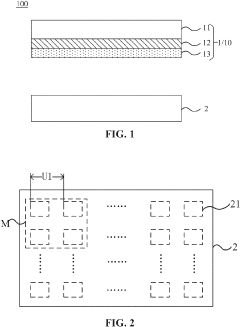
Mass transfer system and mass transfer method
PatentPendingUS20230343891A1
Innovation
- A mass transfer system and method that includes a transfer device and a calibration device with multiple calibration points, where microLEDs are position-calibrated before being transferred to an array substrate through electrical control, allowing for higher transfer rates and yields by using a larger-sized calibration device that can handle more microLEDs at once.
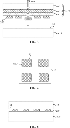
Mass transfer device and mass transfer method
PatentActiveUS11784159B2
Innovation
- A mass transfer device with gradually increasing channels and a method using laser irradiation to separate Micro-LEDs from a first substrate and transfer them through channels to corresponding positions on a second substrate, allowing for a simple and cost-effective adjustment of spacing distances.


Sustainability Impact of Commercial OPV Production
The commercial scale-up of Organic Photovoltaics (OPVs) represents a significant opportunity to advance sustainable energy solutions globally. When evaluating the sustainability impact of commercial OPV production, it becomes evident that these technologies offer substantial environmental advantages compared to traditional silicon-based photovoltaics.
OPV manufacturing processes require significantly lower energy inputs, with energy payback times potentially as short as a few months compared to 1-2 years for silicon panels. This reduced energy requirement translates directly to lower carbon emissions during the production phase. Life cycle assessments indicate that commercial-scale OPV production could achieve carbon footprints 50-80% smaller than conventional PV technologies, depending on manufacturing methods and material choices.
Material sustainability represents another critical advantage of OPV technology. Unlike conventional photovoltaics that rely on rare earth elements and toxic compounds, OPVs primarily utilize carbon-based materials that can be derived from renewable resources. The potential for bio-based precursors further enhances their sustainability profile, creating opportunities for truly circular production systems.
Water consumption in commercial OPV production also demonstrates favorable metrics, with requirements approximately 75% lower than silicon-based alternatives. This reduced water footprint becomes increasingly important as manufacturing scales to gigawatt capacities, particularly in water-stressed regions where renewable energy deployment is critical.
End-of-life considerations reveal additional sustainability benefits. The organic nature of the primary materials enables more straightforward recycling processes, with research demonstrating recovery rates exceeding 90% for key components. Furthermore, the absence of heavy metals and toxic substances simplifies disposal challenges and reduces environmental contamination risks.
From a social sustainability perspective, commercial OPV production presents opportunities for distributed manufacturing models that can support local economies and reduce transportation emissions. The relatively low capital requirements for establishing production facilities, compared to silicon PV manufacturing, enables more geographically diverse production networks.
However, challenges remain in optimizing sustainability across the entire value chain. Current mass transfer challenges in scale-up processes can lead to material waste and efficiency losses that partially offset environmental benefits. Additionally, some specialized additives and processing agents still present environmental concerns that require further innovation to eliminate.
As commercial production scales, continuous sustainability assessment and improvement will be essential to maintain the environmental advantages of OPV technology. Implementing green chemistry principles throughout the manufacturing process and developing closed-loop material systems represent key strategies for maximizing the positive sustainability impact of this promising renewable energy technology.
Cost-Performance Analysis of Scaled OPV Systems
The economic viability of organic photovoltaics (OPV) at commercial scale depends critically on the balance between manufacturing costs and performance metrics. Current cost analyses indicate that scaled OPV systems can achieve production costs between $50-100/m² depending on manufacturing techniques, material selection, and production volume. This represents a significant improvement from earlier generations but remains higher than established silicon-based technologies on a per-watt basis.
Performance degradation during scale-up presents a substantial economic challenge. Laboratory-scale devices typically demonstrate power conversion efficiencies (PCEs) of 14-18%, but these values often decrease to 8-12% in commercial-scale production due to mass transfer limitations affecting film morphology and interfacial properties. This efficiency gap directly impacts the levelized cost of electricity (LCOE), currently estimated at $0.10-0.15/kWh for scaled OPV systems—still above grid parity in many markets.
Material costs constitute approximately 40-60% of total production expenses, with donor-acceptor polymers and fullerene derivatives being particularly cost-intensive. Recent advances in non-fullerene acceptors show promise for reducing material costs while maintaining performance, potentially lowering this proportion to 30-45% of total expenses. Processing costs, including equipment depreciation and energy consumption, account for another 25-35% of production expenses.
Lifetime performance represents another critical economic factor. Current commercial-scale OPV modules demonstrate operational lifetimes of 5-7 years, significantly shorter than the 20-25 years typical of silicon photovoltaics. This shorter lifespan necessitates more frequent replacement, increasing the total cost of ownership despite lower initial installation costs.
Scale economies show promising trends, with production costs potentially decreasing by 15-20% for each doubling of manufacturing capacity. However, these economies of scale are partially offset by increased quality control requirements and yield losses associated with mass transfer challenges in larger production volumes. Current industry data suggests yield rates of 75-85% for commercial-scale production, compared to >95% achievable in laboratory settings.
The integration of OPV into building materials (BIPV) offers a pathway to improved economic viability by serving dual purposes and offsetting construction material costs. Cost-benefit analyses indicate that BIPV applications could reduce the effective cost of OPV systems by 20-30%, significantly enhancing their market competitiveness despite lower efficiencies compared to conventional photovoltaic technologies.
Unlock deeper insights with Patsnap Eureka Quick Research — get a full tech report to explore trends and direct your research. Try now!
Generate Your Research Report Instantly with AI Agent
Supercharge your innovation with Patsnap Eureka AI Agent Platform!