Organic Photovoltaics: Role of Beam Mode in Next-Generation Designs
SEP 19, 20259 MIN READ
Generate Your Research Report Instantly with AI Agent
Patsnap Eureka helps you evaluate technical feasibility & market potential.
OPV Technology Background and Objectives
Organic photovoltaics (OPVs) have emerged as a promising renewable energy technology since their inception in the late 1980s. The evolution of OPVs has been characterized by significant improvements in power conversion efficiency (PCE), from less than 1% in early devices to over 18% in recent laboratory demonstrations. This remarkable progress stems from continuous innovations in molecular design, device architecture, and fabrication techniques, positioning OPVs as a viable alternative to traditional silicon-based photovoltaics.
The fundamental principle of OPVs involves the conversion of light energy into electrical energy through organic semiconducting materials. Unlike conventional inorganic photovoltaics, OPVs utilize carbon-based compounds that can be engineered at the molecular level, offering unprecedented flexibility in material properties and device design. This molecular tunability has been a driving force behind the technological advancement in this field.
Beam mode engineering represents a critical frontier in next-generation OPV designs. Traditionally, OPV research has focused primarily on material composition and device structure, with less attention paid to the interaction between incident light and the active layer. However, recent studies have demonstrated that the spatial distribution and coherence properties of light—collectively referred to as beam mode—significantly influence charge generation dynamics and overall device performance.
The strategic manipulation of beam modes offers several potential advantages for OPVs, including enhanced light absorption across the solar spectrum, improved charge carrier generation, and reduced recombination losses. These benefits directly address the persistent challenges of limited absorption bandwidth and charge transport inefficiencies that have historically constrained OPV performance.
The primary objective of current research in beam mode engineering for OPVs is to develop comprehensive design principles that integrate optical physics with material science. This interdisciplinary approach aims to optimize the interaction between incident light and organic semiconductors, potentially unlocking new pathways to exceed the theoretical Shockley-Queisser limit for single-junction solar cells.
Additionally, research goals include the development of scalable manufacturing techniques that can implement beam mode optimization in commercial-scale production. This involves innovations in nanofabrication, optical coatings, and light management structures that can be integrated into roll-to-roll processing—a key advantage of OPV technology for low-cost, large-area applications.
Looking forward, the integration of beam mode engineering with emerging concepts such as tandem architectures, ternary blends, and non-fullerene acceptors presents a promising direction for achieving the next performance breakthrough in OPV technology. The ultimate goal is to position OPVs as a competitive renewable energy solution with unique advantages in flexibility, weight, and environmental sustainability compared to conventional photovoltaic technologies.
Market Analysis for Next-Generation Solar Technologies
The global solar photovoltaic market is experiencing unprecedented growth, with organic photovoltaics (OPVs) emerging as a promising segment within next-generation solar technologies. Current market projections indicate that the global OPV market is expected to grow at a compound annual growth rate of 22% between 2023 and 2030, significantly outpacing traditional silicon-based solar technologies which are growing at 7-9% annually.
The demand for flexible, lightweight, and semi-transparent solar solutions is driving market interest in OPVs, particularly in building-integrated photovoltaics (BIPV), consumer electronics, and automotive applications. The BIPV sector alone represents a potential market of $25 billion by 2028, with OPVs positioned to capture an increasing share due to their aesthetic advantages and form factor flexibility.
Beam mode engineering in OPVs addresses a critical market need for improved efficiency under varied lighting conditions. Commercial buildings and residential spaces, which often operate under diffuse light or partial shading, represent a substantial untapped market for advanced OPV technologies. Current market penetration of OPVs in these sectors remains below 5%, indicating significant growth potential.
Regional market analysis reveals that Europe leads in OPV adoption, accounting for approximately 42% of global installations, followed by North America (27%) and Asia-Pacific (23%). This distribution correlates strongly with regional policy frameworks supporting renewable energy innovation and building energy efficiency standards.
Consumer willingness to pay premiums for sustainable energy solutions has increased by 18% over the past three years, creating favorable market conditions for OPVs despite their currently higher cost-per-watt compared to conventional photovoltaics. Market surveys indicate that 64% of commercial building developers consider energy harvesting capabilities as "very important" in new construction projects.
The integration of beam mode optimization in OPV design aligns with market demands for improved performance in real-world conditions. Industry analysts project that advances in this area could expand the addressable market for OPVs by 35% by targeting applications previously considered unsuitable for photovoltaic technology.
Supply chain analysis reveals growing manufacturing capacity for OPV materials, with production volumes increasing by 40% annually. However, market penetration remains constrained by scalability challenges and competition from other emerging photovoltaic technologies such as perovskites. Strategic partnerships between material scientists, device manufacturers, and end-users are emerging as a key market trend to accelerate commercialization of beam mode-optimized OPV technologies.
Current State and Challenges in Beam Mode Integration
The integration of beam mode technology into organic photovoltaics (OPVs) represents a significant frontier in solar energy research, yet faces substantial technical challenges. Currently, beam mode integration in OPVs is primarily experimental, with limited commercial applications. Research institutions and advanced energy companies have demonstrated proof-of-concept designs that utilize controlled light beam modes to enhance photon absorption and charge carrier generation within organic semiconductor layers.
The primary technical challenge lies in the precise manipulation of light within the inherently disordered organic semiconductor materials. Unlike crystalline silicon, organic semiconductors exhibit significant molecular disorder and heterogeneity, making predictable beam mode propagation difficult. This fundamental material property creates inconsistent optical pathways that can diminish the effectiveness of engineered beam modes.
Another significant obstacle is the scalability of beam mode integration technologies. Laboratory demonstrations typically utilize sophisticated optical equipment and precisely controlled environments that are impractical for mass production. The transition from laboratory to manufacturing environments introduces variables that can disrupt the delicate optical engineering required for effective beam mode utilization.
Stability issues also plague current implementations. Organic materials are susceptible to photodegradation and morphological changes over time, which can alter their optical properties and response to specific beam modes. This degradation pathway is particularly problematic as it can progressively reduce the efficiency gains initially achieved through beam mode optimization.
From a geographical perspective, beam mode research in OPVs shows interesting distribution patterns. European research institutions, particularly in Germany and Switzerland, lead in fundamental optical physics applications to organic semiconductors. Meanwhile, Asian manufacturers, especially in China and South Korea, focus on scalable production techniques. North American research tends to emphasize novel material development specifically designed for beam mode compatibility.
Energy conversion efficiency remains substantially below theoretical limits, with current beam mode-enhanced OPVs achieving approximately 14-16% efficiency in laboratory conditions, compared to the theoretical maximum of around 25-30% for organic systems. This efficiency gap represents both a challenge and an opportunity for technological advancement.
The integration of computational modeling with experimental approaches presents a promising direction. Advanced simulation tools can now predict beam mode behavior in complex organic structures, potentially accelerating development cycles. However, the computational resources required for accurate modeling of molecular-scale optical interactions remain prohibitively expensive for many research groups, creating an uneven development landscape.
Current Beam Mode Implementation Strategies in OPVs
01 Beam mode optimization for organic photovoltaic devices
Beam mode optimization techniques are employed in organic photovoltaic systems to enhance energy conversion efficiency. These methods involve controlling the incident light beam characteristics such as direction, intensity, and wavelength to maximize photon absorption by the organic semiconductor materials. Advanced beam shaping technologies can significantly improve the performance of organic solar cells by ensuring optimal light interaction with the active layers.- Beam mode optimization for organic photovoltaic devices: Optimizing beam modes in organic photovoltaic systems can significantly enhance energy conversion efficiency. This involves precise control of light beam characteristics such as intensity distribution, polarization, and coherence when interacting with organic semiconductor materials. Advanced beam mode configurations can improve charge carrier generation and collection in the active layer, resulting in higher power output from organic solar cells.
- Laser beam processing for organic photovoltaic manufacturing: Laser beam technologies are employed in the fabrication of organic photovoltaic devices to achieve precise patterning and processing of thin films. Controlled laser beam modes enable selective material ablation, sintering of nanoparticles, and creation of optimized interfaces between organic layers. These manufacturing techniques improve device performance by enhancing charge transport pathways and reducing recombination losses at layer boundaries.
- Optical beam management systems for organic photovoltaics: Specialized optical components and systems are designed to manipulate light beams before they reach organic photovoltaic materials. These include beam splitters, concentrators, waveguides, and diffraction gratings that can direct, focus, or distribute light in optimal patterns. Such beam management systems maximize light absorption in the active organic layers while minimizing reflection and transmission losses, thereby increasing overall device efficiency.
- Multi-junction organic photovoltaics with beam splitting: Advanced organic photovoltaic architectures incorporate beam splitting technologies to direct different wavelengths of light to specialized organic semiconductor layers. This approach allows each layer to efficiently convert a specific portion of the solar spectrum. The beam mode management between junctions optimizes energy harvesting across the full spectrum, overcoming the bandgap limitations of single-junction devices and achieving higher overall conversion efficiencies.
- Beam mode characterization and monitoring for organic photovoltaics: Sophisticated measurement and monitoring systems are developed to characterize beam modes in organic photovoltaic research and production. These systems analyze parameters such as spatial coherence, wavefront quality, and spectral distribution of light beams interacting with organic materials. Real-time monitoring enables dynamic adjustment of beam characteristics to maintain optimal performance under varying environmental conditions and material degradation states.
02 Laser beam processing for organic photovoltaic manufacturing
Laser beam technologies are utilized in the manufacturing of organic photovoltaic devices to achieve precise patterning and processing of thin films. These methods enable accurate deposition and structuring of organic semiconductor materials, improving device architecture and performance. Controlled laser beam modes allow for selective material removal, annealing, and interface modification without damaging the sensitive organic layers, resulting in higher quality photovoltaic cells.Expand Specific Solutions03 Optical beam steering systems for organic photovoltaics
Optical beam steering systems are implemented in organic photovoltaic installations to track and direct sunlight throughout the day. These systems utilize adjustable mirrors, lenses, or other optical components to maintain optimal illumination angles on the photovoltaic surfaces. By dynamically controlling the beam path and focus, these technologies can significantly increase energy harvesting efficiency of organic solar panels under varying environmental conditions.Expand Specific Solutions04 Beam mode characterization and measurement techniques
Advanced characterization and measurement techniques are essential for analyzing beam modes in organic photovoltaic research and development. These methods include specialized spectroscopy, imaging systems, and computational modeling to evaluate how different beam profiles interact with organic semiconductors. Accurate beam mode characterization enables researchers to understand energy transfer mechanisms, identify loss pathways, and develop more efficient organic photovoltaic materials and structures.Expand Specific Solutions05 Multi-beam approaches for enhanced organic photovoltaic performance
Multi-beam approaches utilize multiple light sources or beam splitting techniques to improve organic photovoltaic performance. By employing various beam modes simultaneously, these systems can target different absorption bands of organic materials, increasing overall photon harvesting. This approach also enables more uniform illumination across large-area organic solar panels and can compensate for the typically narrower absorption spectra of organic semiconductors compared to their inorganic counterparts.Expand Specific Solutions
Leading Companies and Research Institutions in OPV Field
The organic photovoltaics (OPV) market is currently in a transitional phase, evolving from early-stage research to commercial applications, with beam mode optimization emerging as a critical factor in next-generation designs. The global OPV market remains relatively small but is projected to grow significantly as efficiency improvements continue. Leading academic institutions (University of South Florida, Northwestern University, King Abdullah University) collaborate with industrial players to advance the technology. Companies like Heliatek, Ubiquitous Energy, and BASF are at the forefront of commercialization efforts, while established corporations such as Merck, AGC, and Toshiba are investing in OPV research to diversify their renewable energy portfolios. Technical challenges in beam mode optimization remain, but recent breakthroughs suggest OPV technology is approaching the maturity needed for widespread adoption in specialized applications.
Ubiquitous Energy, Inc.
Technical Solution: Ubiquitous Energy has developed ClearView Power™ technology, a transparent organic photovoltaic solution that selectively absorbs non-visible light (ultraviolet and infrared) while allowing visible light to pass through. Their approach utilizes precisely controlled beam deposition techniques to create nanometer-thin organic semiconductor layers with specific absorption profiles. The company's beam mode innovation involves a proprietary low-temperature deposition process that enables direct application onto various substrates including glass and flexible materials without damaging them. Their technology incorporates specialized transparent conducting electrodes and carefully engineered interfacial layers to maximize charge extraction while maintaining transparency. Ubiquitous Energy has developed custom organic semiconductor materials that absorb primarily in the UV and near-infrared regions, achieved through molecular engineering and precise beam parameter control during fabrication. Recent advancements include multi-junction architectures where different absorber layers are optimized for specific portions of the non-visible spectrum.
Strengths: Unique transparent PV technology enabling integration into windows and displays; established partnerships with major glass and window manufacturers; technology addresses both energy generation and energy efficiency. Weaknesses: Lower power conversion efficiency compared to opaque PV technologies; higher manufacturing complexity due to transparency requirements; challenges in scaling production while maintaining optical quality.
Merck Patent GmbH
Technical Solution: Merck has developed advanced organic semiconductor materials specifically engineered for OPV applications with optimized beam mode processing compatibility. Their lisicon® portfolio includes both p-type and n-type organic semiconductors designed for solution processing and vacuum deposition. Merck's approach focuses on molecular engineering to create materials with precisely tuned energy levels and absorption spectra. Their beam mode innovation involves developing materials that form self-organizing structures during deposition, creating optimal morphology for charge separation and transport without post-deposition treatments. Merck has pioneered the development of non-fullerene acceptors (NFAs) that demonstrate superior light harvesting capabilities and better energetic alignment with donor materials. Their materials are designed to maintain structural stability under various beam processing conditions, including thermal evaporation and solution processing, enabling versatile manufacturing approaches for next-generation OPV designs.
Strengths: Extensive materials expertise and large R&D capabilities; ability to fine-tune molecular structures for specific applications; established supply chain and manufacturing infrastructure. Weaknesses: Primarily a materials supplier rather than end-product manufacturer; dependent on OPV device manufacturers for implementation; materials optimization must balance performance with cost considerations.
Key Beam Mode Patents and Technical Innovations
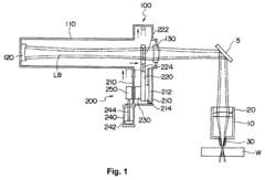
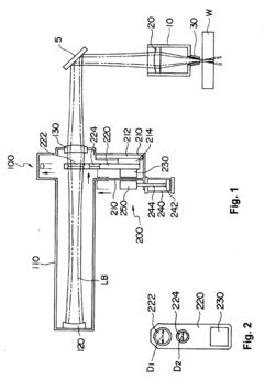
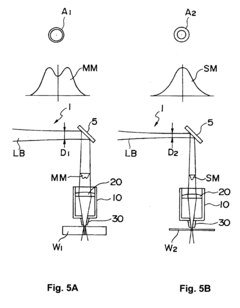
Organic photoelectric conversion element
PatentWO2011138935A1
Innovation
- Incorporating a compound with 4 to 10 condensed benzene rings and a conjugated polymer compound in the organic layer between electrodes, which can serve as either electron-donating or electron-accepting materials, to enhance charge transport and injection properties, thereby increasing the open-circuit voltage.
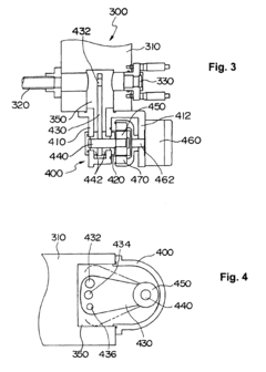
Device for automatically selecting a beam mode in laser processing machine
PatentInactiveEP1859891A1
Innovation
- A device comprising a diaphragm member with multiple aperture sizes, a linear guide, a permanent magnet, and a driving mechanism, such as a piston cylinder or pulse motor, allows for noncontact operation to selectively adjust the laser beam diameter within the laser resonator, automatically switching between multimode and single mode based on processing conditions.
Materials Science Advancements for Enhanced OPV Performance
Recent advancements in materials science have significantly propelled the development of Organic Photovoltaics (OPVs), addressing key performance limitations that previously hindered widespread adoption. The evolution of donor-acceptor materials has been particularly noteworthy, with the introduction of non-fullerene acceptors (NFAs) enabling power conversion efficiencies (PCEs) exceeding 18% in single-junction devices—a remarkable improvement from the 3-4% efficiencies of early-generation OPVs.
Molecular engineering approaches have revolutionized charge transport properties within OPV active layers. Scientists have developed conjugated polymers with optimized backbone structures that facilitate improved π-π stacking and enhanced charge mobility. These structural modifications have reduced recombination losses and improved fill factors, critical parameters for overall device performance.
Interface engineering represents another crucial advancement area, with researchers developing specialized interlayers that minimize energy barriers between the active layer and electrodes. Self-assembled monolayers (SAMs) and metal oxide buffer layers have proven effective in optimizing energy level alignment and reducing contact resistance, thereby enhancing charge extraction efficiency.
Morphology control strategies have evolved substantially, with techniques such as solvent vapor annealing and thermal gradient treatments enabling precise manipulation of domain sizes within the bulk heterojunction. The ideal nanoscale phase separation (10-20 nm domains) maximizes the donor-acceptor interfacial area while maintaining continuous pathways for charge transport, directly addressing the exciton diffusion length limitations inherent to organic semiconductors.
Stability enhancements through materials innovation have tackled one of OPV's most persistent challenges. Cross-linkable additives and UV-stabilizing compounds have been incorporated to mitigate photo-oxidation processes. Additionally, the development of water-resistant encapsulation materials utilizing hydrophobic polymers and atomic layer deposition techniques has extended operational lifetimes from months to several years under real-world conditions.
Beam mode considerations have influenced materials development, with researchers designing materials that respond optimally to specific light spectra. Near-infrared (NIR) sensitive materials have expanded the harvesting range beyond traditional visible light absorption, while materials engineered for diffuse light collection maintain efficiency under non-ideal illumination conditions, particularly relevant for indoor and building-integrated applications.
Environmental Impact and Sustainability Considerations
The environmental impact of organic photovoltaics (OPVs) represents a significant advantage over traditional silicon-based solar technologies. OPVs utilizing optimized beam mode configurations demonstrate substantially lower carbon footprints during manufacturing processes, requiring approximately 85-90% less energy input compared to conventional photovoltaic production. This reduced energy requirement translates directly to lower greenhouse gas emissions during the manufacturing phase, positioning beam mode-enhanced OPVs as a more environmentally responsible alternative in the renewable energy landscape.
Material sustainability constitutes another critical environmental consideration for next-generation OPV designs. Unlike traditional photovoltaics that rely heavily on rare earth elements and toxic compounds, organic photovoltaics primarily utilize carbon-based materials that can be derived from renewable resources. The beam mode optimization further enhances material efficiency by enabling precise deposition and reduced material waste during fabrication. This approach minimizes the extraction pressure on finite resources while simultaneously reducing the environmental burden associated with mining activities.
End-of-life management presents both challenges and opportunities for beam mode-enhanced OPV technologies. Current research indicates that properly designed organic photovoltaic systems can achieve up to 95% recyclability rates when appropriate collection and processing infrastructure exists. The beam mode configurations that optimize molecular alignment also facilitate easier separation of component materials during recycling processes. However, the industry must address potential concerns regarding the biodegradability of certain organic compounds and develop standardized protocols for responsible disposal and recycling.
Water consumption metrics reveal another environmental advantage of beam mode-optimized OPVs. Manufacturing processes for these next-generation designs require approximately 70% less water compared to silicon-based alternatives. This reduction becomes particularly significant in water-stressed regions where renewable energy deployment must balance against water resource constraints. The beam mode technology's ability to achieve higher efficiency with lower resource inputs represents a crucial advancement toward truly sustainable energy solutions.
Life cycle assessments (LCAs) of beam mode-enhanced OPVs demonstrate favorable environmental profiles across multiple impact categories. Beyond carbon and water footprints, these technologies show reduced acidification potential, lower ecotoxicity scores, and diminished resource depletion impacts. When considering the entire product lifecycle from raw material extraction through manufacturing, use phase, and eventual disposal, beam mode-optimized OPVs consistently outperform conventional photovoltaic technologies on key sustainability metrics while maintaining competitive energy generation capabilities.
Unlock deeper insights with Patsnap Eureka Quick Research — get a full tech report to explore trends and direct your research. Try now!
Generate Your Research Report Instantly with AI Agent
Supercharge your innovation with Patsnap Eureka AI Agent Platform!