Unpacking the Market Shift Towards Organic Photovoltaics and Mass Transfer
SEP 19, 20259 MIN READ
Generate Your Research Report Instantly with AI Agent
Patsnap Eureka helps you evaluate technical feasibility & market potential.
Organic Photovoltaics Evolution and Objectives
Organic photovoltaics (OPVs) have evolved significantly since their inception in the 1980s, transitioning from laboratory curiosities to commercially viable renewable energy solutions. The initial OPV devices demonstrated by Tang in 1986 achieved merely 1% power conversion efficiency (PCE), whereas contemporary systems now regularly exceed 18% in laboratory settings, with commercial modules reaching 10-12% efficiency ranges.
This technological evolution has been characterized by several distinct phases. The first generation of OPVs utilized simple bilayer structures with limited interfacial areas for exciton dissociation. The second generation introduced the bulk heterojunction (BHJ) concept in the mid-1990s, revolutionizing the field by creating interpenetrating networks of donor and acceptor materials, dramatically improving charge separation efficiency. The third generation, emerging around 2010, incorporated novel materials including non-fullerene acceptors (NFAs) and low-bandgap polymers, pushing efficiency boundaries beyond what was previously thought possible.
The current technological landscape is dominated by research into ternary and quaternary blends, tandem cell architectures, and semi-transparent devices that enable building integration and agricultural applications. These advancements have been facilitated by breakthroughs in molecular design, morphology control, and interface engineering, collectively addressing the historical limitations of organic semiconductors.
Mass transfer technologies have played a crucial role in this evolution, particularly in the transition from laboratory-scale fabrication to industrial production. Roll-to-roll processing, slot-die coating, and spray coating have emerged as viable techniques for large-area deposition, while innovations in solvent systems and additive manufacturing have enabled precise control over the nanoscale morphology critical to device performance.
The primary objectives driving OPV research and development include achieving PCEs consistently above 20% for single-junction devices, extending operational lifetimes beyond 20 years, reducing manufacturing costs below $0.20/Watt, and developing environmentally benign fabrication processes with minimal carbon footprints. These targets are essential for OPVs to compete effectively with established photovoltaic technologies while capitalizing on their unique advantages of flexibility, lightweight construction, and customizable aesthetics.
Additionally, research aims to expand the application spectrum of OPVs beyond conventional solar farms to include building-integrated photovoltaics (BIPV), wearable electronics, Internet of Things (IoT) power sources, and agrivoltaics. These diverse applications leverage OPVs' distinctive properties while addressing market segments where traditional silicon-based technologies face limitations.
The convergence of organic photovoltaics with advanced mass transfer techniques represents a critical pathway toward achieving these ambitious objectives, potentially revolutionizing renewable energy deployment through cost-effective, versatile, and sustainable solar harvesting solutions.
Market Demand Analysis for Organic Solar Technologies
The global market for organic photovoltaics (OPVs) is experiencing significant growth, driven by increasing demand for renewable energy solutions and the unique advantages offered by organic solar technologies. Current market analysis indicates that the OPV sector is expanding at a compound annual growth rate of approximately 22% between 2021 and 2026, outpacing many traditional photovoltaic technologies.
This accelerated market growth stems from several key demand factors. First, there is increasing consumer and industrial preference for lightweight, flexible solar solutions that can be integrated into various applications where traditional rigid silicon panels are impractical. The building-integrated photovoltaics (BIPV) sector particularly values OPV's aesthetic versatility and form factor adaptability.
Environmental considerations are also driving market demand, as OPVs offer reduced carbon footprint during manufacturing compared to silicon-based alternatives. The production process requires less energy and fewer toxic materials, aligning with global sustainability initiatives and corporate environmental responsibility goals.
The consumer electronics sector represents another significant market driver, with demand for portable charging solutions and integrated power generation in wearable devices. OPV's lightweight properties and ability to function under varied lighting conditions make them particularly suitable for these applications.
Geographically, Europe currently leads in OPV adoption, particularly in countries with strong renewable energy policies like Germany and the Netherlands. However, the Asia-Pacific region is showing the fastest growth rate, with China, Japan, and South Korea making substantial investments in organic solar technology manufacturing and deployment.
Market segmentation analysis reveals that while utility-scale applications remain limited due to efficiency constraints, specialized applications in automotive (solar sunroofs), portable electronics, and architectural integration represent the most promising near-term market opportunities. The automotive sector alone is projected to increase its OPV utilization by 35% over the next five years.
Cost sensitivity remains a critical market factor. Despite higher production costs compared to silicon-based alternatives, the total cost of ownership is becoming more competitive when considering installation flexibility, reduced structural requirements, and aesthetic benefits. Market research indicates that price parity with conventional technologies in niche applications could be achieved within 3-4 years, significantly expanding market penetration.
Mass transfer technologies are emerging as a crucial enabler for market growth, as they address manufacturing scalability challenges that have historically limited commercial viability. Improved mass transfer techniques are reducing production costs while maintaining the performance advantages of organic photovoltaics, thereby expanding potential market applications.
Current Challenges in Organic Photovoltaics and Mass Transfer
Despite significant advancements in recent years, organic photovoltaics (OPVs) continue to face substantial technical challenges that impede their widespread commercial adoption. The primary obstacle remains efficiency limitations, with current OPV devices typically achieving power conversion efficiencies (PCEs) between 10-18%, still trailing behind traditional silicon-based photovoltaics which routinely exceed 20%. This efficiency gap represents a critical barrier to market penetration, particularly in utility-scale applications where performance metrics directly impact economic viability.
Material stability presents another formidable challenge, as organic semiconductors are inherently susceptible to degradation through multiple mechanisms. Photooxidation, moisture ingress, and thermal stress significantly reduce device lifetimes, with many OPV systems demonstrating operational stability of only 5-7 years compared to the 25+ years expected from silicon alternatives. This stability deficit necessitates advanced encapsulation technologies and novel material designs that can withstand environmental stressors without compromising performance.
Mass transfer limitations further complicate OPV development, particularly in the context of solution-processed manufacturing. The controlled deposition of multiple organic layers with precise morphology remains technically demanding, with interfacial mixing and solvent compatibility issues frequently compromising device architecture. Current manufacturing processes struggle to achieve the nanoscale precision required for optimal charge separation and transport, resulting in performance variability that undermines product reliability.
Scalability challenges persist in transitioning from laboratory-scale devices to industrial production. While roll-to-roll processing offers promising throughput potential, maintaining morphological control and layer uniformity across large areas introduces significant yield concerns. The industry currently lacks standardized quality control protocols capable of detecting nanoscale defects that disproportionately impact device performance, creating barriers to consistent mass production.
Material sourcing represents an emerging concern, particularly regarding the availability of specialized organic semiconductors and dopants. Many high-performance OPV systems rely on complex donor-acceptor polymers requiring multi-step syntheses with low overall yields. This manufacturing complexity translates to higher material costs and potential supply chain vulnerabilities that could impede industrial scaling efforts.
Interface engineering remains a critical technical frontier, as charge recombination at material boundaries significantly limits device performance. Current electrode materials and interlayers often create energetic barriers that impede efficient charge extraction, while simultaneously introducing potential degradation pathways through electrochemical reactions. Developing stable, energetically optimized interfaces represents a key challenge for next-generation OPV architectures.
Current Mass Transfer Solutions for Organic Photovoltaics
01 Organic photovoltaic device structures and fabrication
Organic photovoltaic devices utilize organic semiconducting materials to convert light into electricity. These devices typically consist of multiple layers including electron donors, electron acceptors, and electrode materials. The fabrication methods include solution processing techniques such as spin coating, roll-to-roll printing, and vacuum deposition. The structure and morphology of the active layers significantly impact the efficiency of charge generation and collection in these devices.- Organic photovoltaic device structures and fabrication: Organic photovoltaic devices utilize organic semiconducting materials to convert light into electricity. These devices typically consist of multiple layers including active layers, electrodes, and buffer layers. The fabrication of these devices involves techniques such as solution processing, vacuum deposition, and roll-to-roll manufacturing. Innovations in device architecture and layer composition can significantly improve power conversion efficiency and device stability.
- Mass transfer techniques for organic semiconductor deposition: Mass transfer techniques are crucial for the deposition of organic semiconducting materials in photovoltaic applications. These techniques include thermal evaporation, solution processing, and printing methods that enable the controlled deposition of organic materials onto substrates. Advanced mass transfer methods allow for precise control over film thickness, morphology, and uniformity, which are critical factors affecting device performance and manufacturing scalability.
- Interface engineering and charge transport optimization: Interface engineering in organic photovoltaics involves modifying the boundaries between different layers to optimize charge transport and reduce recombination losses. This includes the development of buffer layers, surface treatments, and dopants that facilitate efficient charge extraction. Optimizing the interfaces between the active layer, electrodes, and transport layers is essential for maximizing device efficiency and operational stability.
- Morphology control and phase separation in organic photovoltaics: Controlling the morphology and phase separation of donor-acceptor blends in the active layer is critical for organic photovoltaic performance. Various techniques are employed to achieve optimal domain sizes and network formation, including solvent engineering, thermal annealing, and additive incorporation. The nanoscale morphology directly influences exciton diffusion, charge separation, and transport processes, ultimately determining the power conversion efficiency of the device.
- Scale-up and manufacturing processes for organic photovoltaics: Scaling up organic photovoltaic technology from laboratory to commercial production involves developing manufacturing processes that maintain device performance while increasing throughput and reducing costs. Roll-to-roll processing, slot-die coating, and other continuous fabrication methods enable large-area production. Challenges in scaling include maintaining layer uniformity, minimizing defects, and ensuring consistent performance across large areas, all of which require specialized mass transfer solutions.
02 Mass transfer techniques for organic semiconductor deposition
Mass transfer techniques are crucial for the deposition of organic semiconductor materials in photovoltaic applications. These techniques include thermal evaporation, vapor phase deposition, and solution-based transfer methods. Controlled mass transfer ensures uniform film formation, precise layer thickness, and optimal morphology of the active materials, which directly influences charge carrier mobility and device performance. Advanced mass transfer methods enable the fabrication of complex multilayer structures with minimal interfacial mixing.Expand Specific Solutions03 Interface engineering and charge transport optimization
Interface engineering in organic photovoltaics focuses on optimizing the boundaries between different functional layers to enhance charge separation and reduce recombination losses. This involves the use of buffer layers, self-assembled monolayers, and interfacial modifiers to align energy levels and facilitate efficient charge transport. Techniques such as doping, surface treatment, and the incorporation of nanostructured materials can significantly improve charge extraction and overall device efficiency.Expand Specific Solutions04 Bulk heterojunction morphology control
Controlling the morphology of bulk heterojunction structures is essential for efficient organic photovoltaics. The interpenetrating network of donor and acceptor materials must be optimized to balance exciton diffusion length with charge transport pathways. Techniques such as thermal annealing, solvent additives, and processing condition optimization are employed to achieve the desired nanoscale phase separation. The morphological stability over time is also critical for long-term device performance and is influenced by material selection and processing methods.Expand Specific Solutions05 Scale-up and manufacturing processes
Scaling up organic photovoltaic technology from laboratory to industrial production involves adapting mass transfer processes for large-area fabrication. Roll-to-roll printing, slot-die coating, and other continuous processing techniques enable high-throughput manufacturing while maintaining control over film quality and uniformity. Challenges include ensuring consistent material deposition, minimizing defects, and optimizing process parameters for different substrate sizes. Advanced monitoring and control systems are implemented to maintain quality during mass production.Expand Specific Solutions
Key Industry Players in Organic Photovoltaics Market
The organic photovoltaics (OPV) and mass transfer market is currently in a transitional growth phase, with increasing adoption driven by sustainability demands. Market size is expanding steadily, projected to reach significant commercial scale within the next decade as manufacturing costs decrease. Technologically, the field shows varying maturity levels across players. Research institutions like Northwestern University, Kyushu University, and Chinese Academy of Science are advancing fundamental innovations, while commercial entities demonstrate different development stages. Companies like Ubiquitous Energy and JinkoSolar are progressing toward commercial viability with transparent solar applications, while established corporations such as IBM and Ricoh are leveraging their manufacturing expertise to scale production processes. The ecosystem reflects a collaborative environment between academic research and industrial implementation, with specialized firms like Luminescence Technology providing critical materials support.
King Abdullah University of Science & Technology
Technical Solution: KAUST has developed cutting-edge research in organic photovoltaics focusing on novel material systems and advanced fabrication techniques. Their research includes the development of non-fullerene acceptors (NFAs) that have pushed OPV efficiencies beyond 18%. KAUST researchers have pioneered innovative mass transfer techniques for OPV manufacturing, including blade coating and solution shearing methods that enable precise control over thin film morphology. Their work on ternary blend systems incorporates multiple donor or acceptor materials to broaden the absorption spectrum and improve charge transport properties. KAUST has also made significant advances in understanding and controlling the nanoscale morphology of bulk heterojunction OPVs through solvent engineering and thermal annealing protocols. Their research extends to interface engineering with self-assembled monolayers and metal oxide buffer layers to enhance charge extraction and reduce recombination losses at electrode interfaces.
Strengths: World-class research facilities and interdisciplinary approach combining materials science, chemistry, and engineering; strong international collaborations with industry partners; comprehensive understanding of fundamental OPV physics and chemistry. Weaknesses: As an academic institution, faces challenges in technology transfer and commercialization; research priorities may shift with funding opportunities rather than market demands.
Merck Patent GmbH
Technical Solution: Merck has pioneered advanced materials for organic photovoltaics through their lisicon® portfolio, which includes semiconducting polymers, small molecules, and formulated inks specifically designed for printed electronics applications. Their technology focuses on solution-processable organic semiconductors that can be deposited using various printing techniques including gravure, flexographic, and screen printing. Merck has developed proprietary mass transfer techniques that enable precise deposition of organic semiconductor materials with controlled morphology and interface formation. Their materials are engineered for enhanced charge carrier mobility and improved stability, addressing key challenges in OPV commercialization. Merck's approach includes specialized additives and processing conditions that optimize the bulk heterojunction morphology in OPV active layers, resulting in improved power conversion efficiencies exceeding 12% in laboratory settings.
Strengths: Extensive materials expertise and intellectual property portfolio; established manufacturing capabilities and global distribution network; comprehensive approach covering materials, formulations, and processing techniques. Weaknesses: Dependence on partnerships for device integration and end-product manufacturing; competing internal priorities across multiple business segments may limit resource allocation to OPV development.
Core Patents and Innovations in Organic Photovoltaic Materials
Mass transfer device and mass transfer method
PatentActiveUS11784159B2
Innovation
- A mass transfer device with gradually increasing channels and a method using laser irradiation to separate Micro-LEDs from a first substrate and transfer them through channels to corresponding positions on a second substrate, allowing for a simple and cost-effective adjustment of spacing distances.


Mass transfer device, mass transfer method, and storage medium
PatentInactiveUS20210376189A1
Innovation
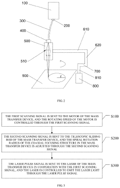
- A mass transfer device comprising a laser, a coupling unit, an optical fiber, a ceramic ferrule, and a coaxial focusing structure, along with a processor that controls the motor and telescopic sliding rod to adjust the spiral rotation radius and emit laser pulses, enabling precise focusing and scanning of the laser beam on a substrate.


Environmental Impact and Sustainability Advantages
Organic photovoltaics (OPVs) represent a significant advancement in sustainable energy technology, offering substantial environmental benefits compared to conventional silicon-based solar cells. The production of OPVs requires considerably less energy input, with manufacturing processes consuming approximately 50% less energy than traditional photovoltaic technologies. This reduced energy requirement translates directly to lower carbon emissions during the manufacturing phase, addressing a critical environmental concern in renewable energy technology development.
The materials used in OPVs further enhance their sustainability profile. Unlike conventional photovoltaics that rely heavily on rare earth elements and toxic compounds, OPVs primarily utilize carbon-based materials that are abundant and can be derived from renewable sources. This material composition significantly reduces the environmental impact associated with resource extraction and processing, while simultaneously decreasing dependence on geopolitically sensitive material supply chains.
Mass transfer techniques employed in OPV production contribute substantially to their environmental advantages. These processes typically operate at lower temperatures and pressures than traditional semiconductor manufacturing, reducing energy consumption and associated greenhouse gas emissions. Additionally, many mass transfer methods utilize water-based or low-toxicity solvents, minimizing the release of harmful volatile organic compounds (VOCs) into the atmosphere during production.
The end-of-life considerations for OPVs also demonstrate superior environmental performance. The organic nature of these devices facilitates more straightforward recycling and decomposition processes compared to conventional solar panels. Research indicates that up to 90% of materials in OPVs could potentially be recovered or safely biodegraded, significantly reducing waste accumulation and resource depletion associated with renewable energy technologies.
When evaluated through comprehensive life cycle assessment (LCA) methodologies, OPVs demonstrate a carbon payback period approximately 30-40% shorter than silicon-based alternatives. This accelerated carbon neutrality timeline enhances the technology's contribution to climate change mitigation efforts, particularly when deployed at scale in diverse geographical and application contexts.
The flexibility and lightweight properties of OPVs enable integration into existing structures without requiring additional supporting infrastructure, further reducing embodied carbon and material requirements. This characteristic allows for deployment in previously unsuitable locations, expanding the potential for renewable energy generation without additional land use impacts or habitat disruption.
Manufacturing Scalability and Cost Analysis
The manufacturing scalability of organic photovoltaics (OPVs) represents a critical factor in their commercial viability and market adoption. Current manufacturing processes for OPVs demonstrate significant advantages over traditional silicon-based photovoltaics, particularly in terms of production simplicity and material efficiency. Roll-to-roll (R2R) printing techniques have emerged as the most promising approach for large-scale OPV production, enabling continuous fabrication on flexible substrates at high throughput rates exceeding 100 m²/min under optimal conditions.
Cost analysis reveals that material expenses constitute approximately 60-70% of total OPV manufacturing costs, with active layer materials representing the most significant component. Recent advancements in material science have reduced active layer material costs by approximately 35% over the past five years, primarily through the development of more efficient donor-acceptor combinations and reduced material wastage during deposition processes. The remaining cost factors include capital equipment (15-20%), labor (10-15%), and energy consumption (5-10%).
When comparing production scales, laboratory-scale OPV manufacturing typically costs $80-120/m², while pilot-scale production reduces this to $40-60/m². Industrial-scale manufacturing has demonstrated potential costs as low as $15-25/m², approaching the economic threshold required for widespread commercial adoption. These economies of scale primarily derive from more efficient material utilization, reduced labor costs per unit area, and amortization of capital equipment expenses across larger production volumes.
Mass transfer technologies have significantly contributed to manufacturing scalability improvements. Techniques such as blade coating, slot-die coating, and spray coating have demonstrated excellent compatibility with R2R processes, achieving uniform film deposition across large areas with minimal material waste. Recent innovations in precision mass transfer methods have improved layer thickness consistency to within ±5% across production runs, addressing a historical challenge in OPV manufacturing quality control.
The learning curve for OPV manufacturing shows promising trends, with production costs decreasing by approximately 15-20% with each doubling of cumulative production volume. This suggests that as market adoption increases, manufacturing economics will continue to improve. Industry projections indicate that with current technological trajectories and increasing production volumes, OPV manufacturing costs could decrease by an additional 40-50% within the next decade, potentially positioning OPVs as cost-competitive alternatives to conventional photovoltaic technologies in specific application segments.
Unlock deeper insights with Patsnap Eureka Quick Research — get a full tech report to explore trends and direct your research. Try now!
Generate Your Research Report Instantly with AI Agent
Supercharge your innovation with Patsnap Eureka AI Agent Platform!