Emerging Quantum Interconnects in Nano-fabricated Devices
SEP 29, 20259 MIN READ
Generate Your Research Report Instantly with AI Agent
Patsnap Eureka helps you evaluate technical feasibility & market potential.
Quantum Interconnect Evolution and Objectives
Quantum interconnects represent a critical frontier in quantum computing, serving as the essential links between quantum processing units. The evolution of these interconnects has been closely tied to advancements in nanofabrication techniques, which have enabled increasingly sophisticated quantum device architectures. Initially, quantum interconnects were primarily conceptual, with early theoretical frameworks emerging in the late 1990s as quantum computing began to transition from purely theoretical to experimental implementations.
The field gained significant momentum in the early 2000s with the development of superconducting quantum circuits, which necessitated reliable interconnection methods between quantum bits. This period marked the transition from isolated quantum elements to the first rudimentary quantum networks. By 2010, researchers had demonstrated coherent coupling between superconducting qubits, representing a crucial milestone in quantum interconnect technology.
Recent years have witnessed exponential growth in quantum interconnect research, driven by the realization that quantum computing scalability fundamentally depends on robust interconnection solutions. The integration of heterogeneous quantum systems—combining different qubit modalities or quantum processors with classical electronics—has emerged as a particularly promising direction, demanding novel interconnect approaches that preserve quantum coherence while facilitating efficient information transfer.
Current technological trajectories suggest several key objectives for quantum interconnect development. Primary among these is maintaining quantum coherence across interconnected systems, as decoherence remains the fundamental challenge limiting quantum computing capabilities. Researchers aim to develop interconnects that minimize decoherence effects while maximizing information transfer fidelity.
Scalability represents another critical objective, with efforts focused on creating architectures that can support thousands or millions of interconnected qubits—essential for fault-tolerant quantum computing. This necessitates interconnect solutions compatible with existing nanofabrication techniques while offering pathways to mass production.
Integration with classical control systems constitutes a third major objective, as practical quantum computers will require seamless interfaces between quantum processing elements and conventional electronic systems for control, measurement, and data extraction. This hybrid integration presents unique challenges for interconnect design.
The field is now moving toward standardized approaches for quantum interconnects, with several competing technologies under investigation. These include photonic links for long-distance quantum communication, superconducting transmission lines for on-chip connectivity, and novel material interfaces for hybrid quantum systems. The ultimate goal remains developing quantum interconnect technologies that enable practical, large-scale quantum computing systems capable of outperforming classical computers in solving previously intractable problems.
Market Demand Analysis for Quantum Computing Infrastructure
The quantum computing infrastructure market is experiencing unprecedented growth, driven by significant advancements in quantum technologies and increasing recognition of their transformative potential across industries. Current market projections indicate that the global quantum computing market, including infrastructure components, is expected to grow from approximately 500 million USD in 2023 to reach 3 billion USD by 2028, representing a compound annual growth rate of over 30%.
Quantum interconnects, particularly those implemented in nano-fabricated devices, represent a critical infrastructure component that addresses the fundamental challenge of scaling quantum systems. The demand for these specialized interconnects stems from the need to maintain quantum coherence while enabling communication between quantum processing units, memory elements, and input/output interfaces.
Financial services, pharmaceuticals, and advanced materials sectors are emerging as primary demand drivers for quantum computing infrastructure. Financial institutions are investing heavily in quantum capabilities for portfolio optimization, risk assessment, and fraud detection applications. The pharmaceutical industry sees quantum computing as revolutionary for drug discovery processes, potentially reducing development timelines from years to months. Materials science companies are exploring quantum simulations to accelerate the discovery of novel materials with specific properties.
Government and defense sectors worldwide are also significant contributors to market demand, with national quantum initiatives launched in the United States, China, European Union, Japan, and other countries. These initiatives collectively represent over 25 billion USD in committed funding over the next decade, with substantial portions allocated to infrastructure development including quantum interconnect technologies.
The enterprise adoption curve shows increasing interest in quantum-ready infrastructure, with approximately 40% of Fortune 500 companies currently engaged in quantum computing exploration or implementation projects. This represents a doubling of enterprise engagement compared to just three years ago, signaling accelerating market demand.
Cloud-based quantum computing services are experiencing particularly strong growth, with major providers reporting subscription increases exceeding 70% year-over-year. This service model is driving demand for scalable quantum infrastructure components that can support distributed quantum computing architectures.
Supply chain constraints present significant challenges to meeting this growing demand. The specialized materials and fabrication processes required for quantum interconnects face limited production capacity, with lead times for certain components extending to 18 months. This supply-demand imbalance is creating premium pricing opportunities for established suppliers while simultaneously attracting new market entrants.
Current Challenges in Nano-fabricated Quantum Interconnects
Despite significant advancements in quantum computing technologies, nano-fabricated quantum interconnects face several critical challenges that impede their widespread implementation and scalability. The primary obstacle remains coherence maintenance across interconnected quantum systems. When quantum information traverses between different components, decoherence occurs rapidly due to environmental interactions, resulting in quantum state degradation before meaningful operations can be completed. This fundamental issue becomes increasingly problematic as system complexity grows.
Material interface challenges present another significant barrier. Quantum interconnects often require joining dissimilar materials with precise atomic alignment. The resulting boundary effects create unpredictable quantum behavior, including energy losses, reflection phenomena, and unwanted state modifications. Current fabrication techniques struggle to achieve the necessary atomic-level precision consistently across large-scale integrated systems.
Thermal management represents a critical engineering challenge. Many quantum systems require near-absolute zero temperatures to maintain quantum states, yet interconnect components can generate localized heating during operation. This thermal gradient disrupts quantum coherence and introduces computational errors. Developing thermally isolated interconnects while maintaining functional connectivity remains an unsolved engineering problem.
Signal fidelity across quantum interconnects suffers from noise susceptibility at the nanoscale. Quantum signals are inherently fragile, and nano-fabricated channels experience various noise sources including electromagnetic interference, thermal fluctuations, and mechanical vibrations. Current error correction techniques require substantial overhead that limits practical implementation in complex systems.
Scalability presents perhaps the most significant challenge for commercial viability. Laboratory demonstrations have achieved functional quantum interconnects between limited numbers of qubits, but scaling to thousands or millions of interconnected quantum elements introduces exponential complexity in fabrication, control, and error management. Current manufacturing approaches cannot economically produce the required precision at scale.
Standardization remains elusive in this rapidly evolving field. Multiple competing approaches to quantum interconnect design—including photonic channels, superconducting waveguides, and spin-based coupling—create a fragmented development landscape. The lack of industry standards impedes collaborative progress and increases development costs as organizations pursue parallel, often incompatible solutions.
Finally, verification and testing methodologies for quantum interconnects remain underdeveloped. Conventional electronic testing equipment and approaches are inadequate for measuring quantum state preservation across interconnects. New measurement techniques that can assess quantum fidelity without disrupting the very states being measured are required but remain in early development stages.
State-of-the-Art Quantum Interconnect Solutions
01 Quantum interconnect architectures
Various architectures for quantum interconnects that enable communication between quantum computing components. These architectures include specialized designs for connecting quantum bits (qubits) across different quantum processing units, allowing for scalable quantum computing systems. The interconnects are designed to maintain quantum coherence while facilitating the transfer of quantum information between separate quantum elements.- Quantum interconnect architectures: Various architectures for quantum interconnects that enable communication between quantum computing components. These architectures include designs for connecting quantum bits (qubits) across different quantum processing units, implementing quantum communication channels, and creating scalable quantum computing systems. The interconnect architectures address challenges such as maintaining quantum coherence during information transfer and minimizing decoherence effects.
- Superconducting quantum interconnects: Superconducting materials and structures used for quantum interconnections that operate at cryogenic temperatures. These interconnects leverage superconducting properties to maintain quantum coherence and facilitate the transmission of quantum information with minimal loss. The designs include superconducting transmission lines, resonators, and coupling elements that enable efficient interaction between quantum components while preserving quantum states.
- Optical quantum interconnects: Optical systems and components designed for quantum interconnection using photons as quantum information carriers. These interconnects utilize optical fibers, waveguides, and photonic integrated circuits to transmit quantum information between distant quantum processors. The optical approach offers advantages for long-distance quantum communication and networking while maintaining the quantum properties necessary for quantum computing operations.
- Fabrication methods for quantum interconnects: Manufacturing techniques and processes specifically developed for creating quantum interconnect structures. These methods address the unique challenges of fabricating quantum-compatible interconnections, including precise material deposition, nanoscale patterning, and integration with conventional electronics. The fabrication approaches ensure the preservation of quantum properties while enabling scalable production of quantum computing systems.
- Quantum-classical interface interconnects: Specialized interconnect technologies that bridge quantum computing elements with classical electronic systems. These hybrid interconnects enable the control and readout of quantum states using conventional electronics while minimizing decoherence effects. The designs include signal conversion mechanisms, isolation techniques to prevent noise from classical systems affecting quantum operations, and efficient data transfer protocols between quantum and classical domains.
02 Superconducting quantum interconnects
Superconducting materials and structures used for quantum interconnections that operate at extremely low temperatures. These interconnects leverage superconducting properties to minimize signal loss and maintain quantum coherence during information transfer. The designs include specialized waveguides, resonators, and transmission lines that can carry quantum information with minimal decoherence, essential for building large-scale quantum computing systems.Expand Specific Solutions03 Optical quantum interconnects
Optical-based systems for quantum interconnection that use photons to transfer quantum information. These interconnects utilize optical fibers, waveguides, and photonic integrated circuits to connect quantum processing units. The optical approach offers advantages in long-distance quantum communication and can interface with different types of quantum computing platforms, enabling hybrid quantum systems.Expand Specific Solutions04 Quantum interconnect fabrication methods
Manufacturing techniques and processes specifically developed for creating quantum interconnects with high precision and reliability. These methods address the challenges of fabricating nanoscale structures that can maintain quantum coherence. The approaches include specialized deposition techniques, lithography processes, and material integration strategies that enable the creation of complex quantum interconnect structures compatible with existing semiconductor fabrication infrastructure.Expand Specific Solutions05 Quantum-classical interface technologies
Technologies that bridge quantum and classical computing domains, allowing for effective control and readout of quantum systems. These interfaces translate between the quantum world of superposition and entanglement and the classical world of binary information. The designs include specialized control electronics, signal conversion systems, and error correction mechanisms that enable classical computers to program, control, and extract results from quantum processors.Expand Specific Solutions
Leading Organizations in Quantum Interconnect Development
Quantum interconnects in nano-fabricated devices are emerging as a critical frontier in quantum computing, currently in the early growth phase with an estimated market size of $500-700 million, projected to expand significantly as quantum technologies mature. The competitive landscape features established tech giants like IBM, Intel, and Samsung Electronics driving commercial development alongside specialized research from academic institutions such as MIT, Rice University, and Cornell. Technical maturity varies across implementations, with superconducting quantum interconnects showing more advancement than photonic or spin-based approaches. Companies like NXP Semiconductors and HP Enterprise are focusing on scalable manufacturing processes, while research institutions like the Naval Research Laboratory and Industrial Technology Research Institute are pioneering fundamental breakthroughs in coherence and fidelity for these interconnects.
Samsung Electronics Co., Ltd.
Technical Solution: Samsung has developed quantum interconnect technologies focusing on semiconductor-based approaches that leverage their expertise in advanced materials and nanofabrication. Their research centers on creating scalable quantum interconnects using silicon-germanium heterostructures that can host spin qubits with improved coherence properties[8]. Samsung's quantum interconnect technology incorporates specialized on-chip microwave transmission lines that enable high-fidelity control signals to reach quantum devices while minimizing thermal loads and electromagnetic interference. They have demonstrated progress in developing cryogenic CMOS electronics that can operate at temperatures compatible with quantum processors, reducing the complexity of interconnects between room temperature control systems and quantum devices[9]. Samsung's Advanced Institute of Technology has also explored quantum interconnects based on topological materials that could potentially enable more robust quantum information transfer resistant to environmental noise. Their approach integrates quantum memory elements with quantum processing units through carefully designed interfaces that preserve quantum coherence while enabling high-bandwidth information exchange.
Strengths: World-class semiconductor manufacturing capabilities; extensive experience with advanced materials engineering; strong vertical integration from materials to systems. Weaknesses: Relatively newer focus on quantum technologies compared to computing giants; less public disclosure of quantum research progress; competing priorities across diverse technology portfolio.
Intel Corp.
Technical Solution: Intel's quantum interconnect technology focuses on spin qubits fabricated using silicon-based semiconductor manufacturing processes. Their approach leverages existing CMOS fabrication techniques to create quantum dots that trap individual electrons, whose spin states represent quantum information. Intel has developed specialized interconnect structures that enable coherent coupling between these spin qubits while maintaining compatibility with their advanced semiconductor manufacturing capabilities[3]. Their Horse Ridge cryogenic control chip represents a significant advancement in quantum interconnect technology, integrating classical control electronics that can operate at cryogenic temperatures close to the quantum processor, reducing the complexity of wiring between room temperature and the quantum system[4]. Intel's quantum interconnects incorporate specialized routing techniques that minimize electromagnetic interference and maintain signal integrity across temperature gradients. Their research includes developing specialized materials and interfaces that can maintain quantum coherence while enabling the high-density integration necessary for practical quantum computing systems.
Strengths: Unparalleled semiconductor manufacturing expertise; potential for leveraging existing fabrication infrastructure; integration of classical and quantum components. Weaknesses: Relatively newer entrant to quantum computing compared to some competitors; spin qubit technology still maturing; challenges in achieving high-fidelity multi-qubit operations at scale.
Key Patents and Research in Nano-fabricated Quantum Links
Bonded structure including a carbon nanotube
PatentInactiveUS20040142172A1
Innovation
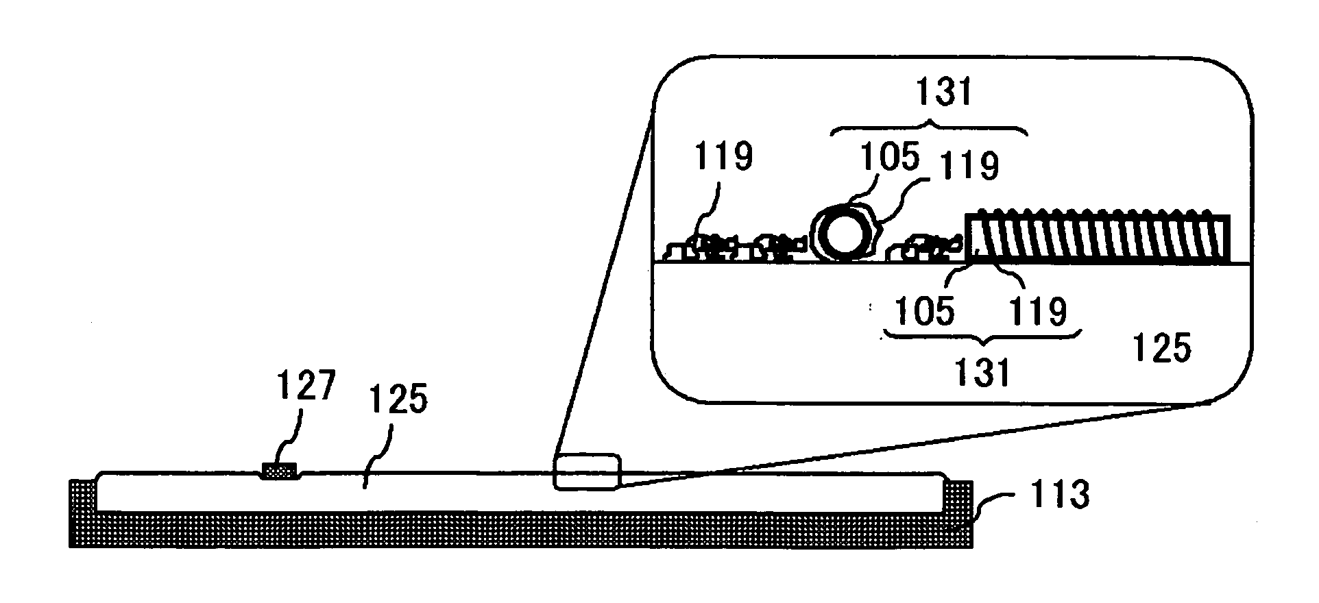
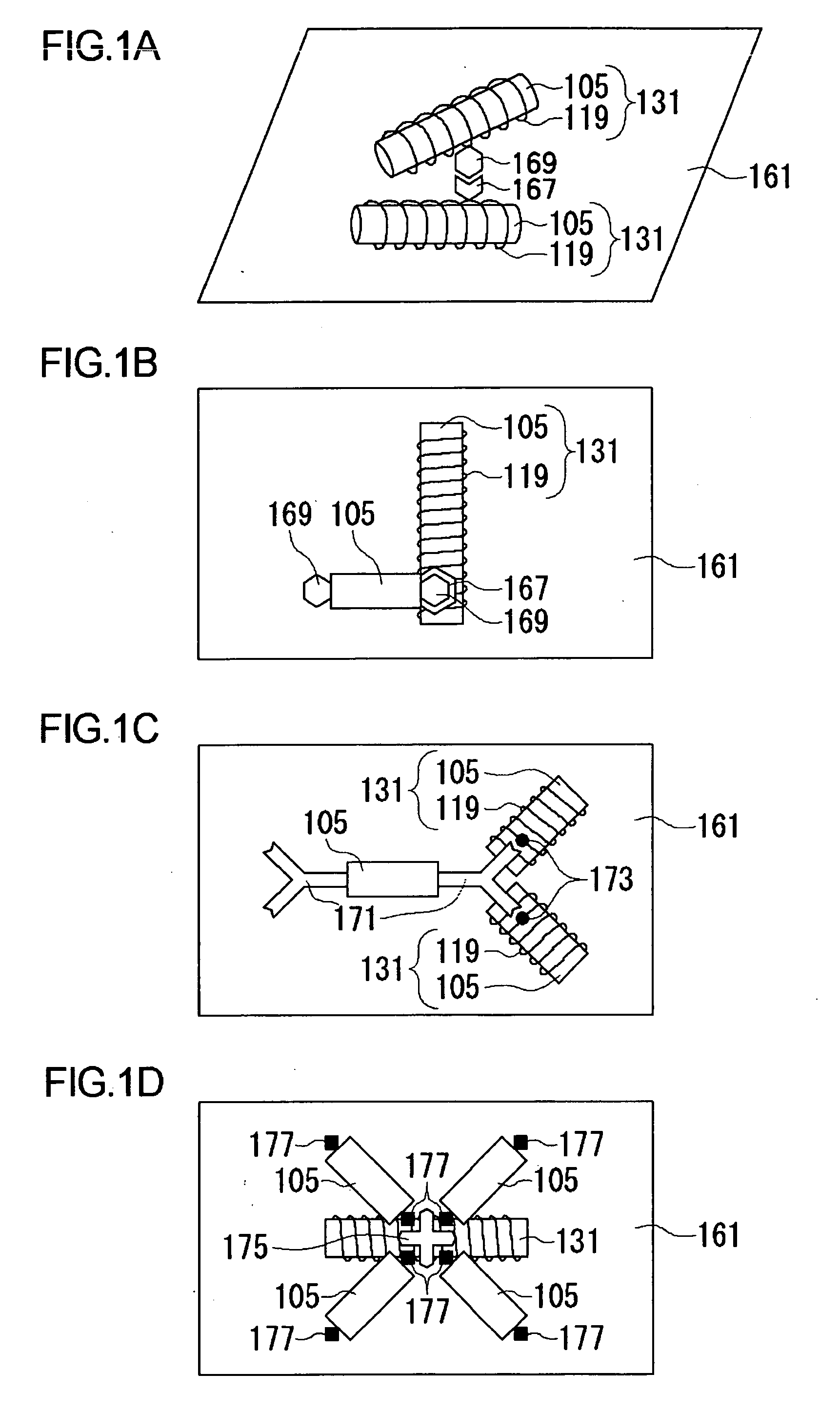
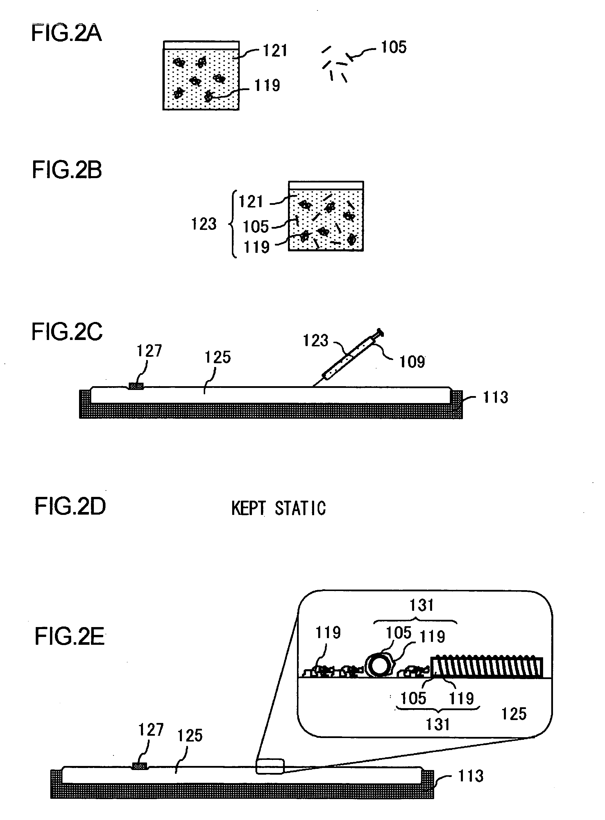
- A bonded structure is formed by wrapping a polymer around the carbon nanotube, which serves as a coating material, allowing for precise control over the thickness and characteristics of the tunnel layer and Coulomb island, enabling stable bonding with other structures and improved performance in nano-devices.
Process for fabricating nanoelectronic device by intermittent exposure
PatentInactiveUS20050139819A1
Innovation
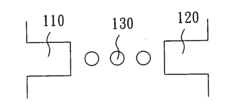
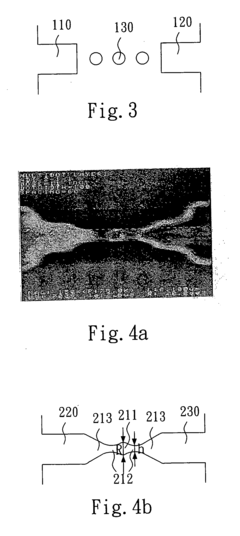
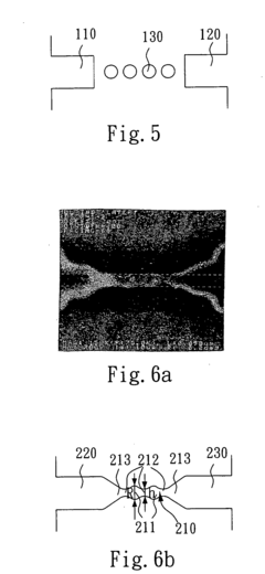
- A process involving intermittent exposure using lithography to form a substrate with noncontinuous quantum dots arranged between electrodes, creating a quantum island group with linked islands and tunnel barriers, allowing for the fabrication of nanoelectronic devices with multiple quantum islands, enabling flexible circuit design and reduced signal interference.
Quantum Error Correction in Interconnect Systems
Quantum Error Correction (QEC) represents a critical frontier in the development of quantum interconnect systems, addressing the fundamental challenge of quantum decoherence. In nano-fabricated quantum devices, interconnects are particularly vulnerable to environmental noise and quantum information degradation. Traditional error correction codes from classical computing prove insufficient due to the unique constraints of quantum mechanics, including the no-cloning theorem and measurement-induced collapse of quantum states.
Recent advancements in surface codes and topological quantum error correction show promising applications for interconnect systems. These approaches leverage redundant physical qubits to encode logical qubits, creating error-resistant information channels between quantum processing units. The distance parameter in these codes directly correlates with error correction capability, with current experimental implementations achieving distances of 5-7 in leading quantum hardware platforms.
Interconnect-specific error correction protocols have emerged as a specialized subfield. These protocols address the unique challenges of quantum state transfer across physical distances while maintaining coherence. Notably, entanglement purification techniques combined with quantum repeater architectures enable long-distance quantum communication with manageable error rates. Recent experiments have demonstrated error-corrected quantum state transfer across chip-scale distances with fidelities exceeding 99%.
Hardware-software co-design approaches are gaining traction in quantum interconnect error correction. Low-level hardware error mitigation techniques, including dynamical decoupling sequences and optimal control theory, complement higher-level QEC codes. This integrated approach has shown a 2-3x improvement in effective coherence times for quantum information traversing nano-fabricated interconnects compared to uncorrected systems.
Material engineering plays a crucial role in reducing the baseline error rates in quantum interconnects. Superconducting transmission lines, silicon photonics waveguides, and spin-based quantum channels each present different error profiles requiring tailored correction strategies. Hybrid approaches combining multiple physical implementations with specialized error correction codes show particular promise for complex quantum networks.
Looking forward, the development of resource-efficient QEC codes specifically optimized for interconnect applications represents a key research direction. Current codes require significant qubit overhead, with logical-to-physical qubit ratios often exceeding 10:1. Reducing this overhead while maintaining error correction capabilities will be essential for scaling quantum interconnect systems to practical applications in distributed quantum computing and quantum networks.
Materials Science Advancements for Quantum Interfaces
Recent advancements in materials science have revolutionized the development of quantum interfaces, particularly for nano-fabricated quantum interconnect devices. The emergence of two-dimensional materials such as graphene, hexagonal boron nitride (h-BN), and transition metal dichalcogenides (TMDs) has provided unprecedented opportunities for creating atomically precise quantum interfaces with minimal decoherence effects.
These 2D materials exhibit exceptional properties including high electron mobility, tunable band gaps, and strong light-matter interactions, making them ideal candidates for quantum information processing applications. Particularly noteworthy is the ability to create van der Waals heterostructures by stacking different 2D materials, enabling precise engineering of quantum states at interfaces without the constraints of lattice matching required in traditional epitaxial growth.
Topological materials represent another significant breakthrough, offering robust quantum states protected against environmental perturbations. Materials such as topological insulators and Weyl semimetals provide naturally occurring quantum channels with reduced backscattering, potentially serving as ideal interconnects between quantum processing units.
Advances in superconducting materials have also contributed substantially to quantum interface development. High-temperature superconductors and novel superconducting thin films with precisely controlled properties enable the creation of Josephson junctions with unprecedented coherence times. Recent work on epitaxial growth of aluminum on semiconductor surfaces has yielded exceptionally clean superconductor-semiconductor interfaces critical for topological quantum computing implementations.
Nanofabrication techniques have evolved in parallel, with atomic layer deposition (ALD) and molecular beam epitaxy (MBE) now capable of creating interfaces with atomic precision. These techniques minimize defects and impurities that would otherwise serve as decoherence sources. Additionally, helium ion microscopy and focused ion beam technologies allow for post-fabrication tuning of quantum interfaces without introducing significant damage.
The integration of ferromagnetic materials with superconductors has opened pathways to novel quantum effects at interfaces, including the generation of Majorana zero modes through proximity effects. These hybrid quantum systems combine the advantages of different material platforms while mitigating their individual limitations, representing a promising direction for scalable quantum technologies.
Unlock deeper insights with Patsnap Eureka Quick Research — get a full tech report to explore trends and direct your research. Try now!
Generate Your Research Report Instantly with AI Agent
Supercharge your innovation with Patsnap Eureka AI Agent Platform!
