Exploring the Dielectric Properties of Magnesium Nitride
AUG 1, 20259 MIN READ
Generate Your Research Report Instantly with AI Agent
Patsnap Eureka helps you evaluate technical feasibility & market potential.
Mg3N2 Dielectric Research Background
Magnesium nitride (Mg3N2) has emerged as a material of significant interest in the field of dielectrics, attracting attention from researchers and industry professionals alike. The exploration of its dielectric properties is rooted in the broader context of the search for novel materials with enhanced performance characteristics for various electronic and optical applications.
The study of Mg3N2's dielectric properties can be traced back to the early 2000s when researchers began to investigate alternative materials for use in electronic devices. As traditional silicon-based technologies approached their physical limits, the need for materials with superior dielectric constants and lower power consumption became increasingly apparent. This led to a surge in research focused on wide-bandgap semiconductors and related compounds, including magnesium nitride.
Mg3N2 belongs to the family of Group III nitrides, which also includes aluminum nitride (AlN) and gallium nitride (GaN). These materials have gained prominence due to their excellent thermal stability, wide bandgap, and potential for high-frequency applications. The unique crystal structure of Mg3N2, with its anti-bixbyite arrangement, contributes to its distinct electronic and optical properties, making it a promising candidate for dielectric applications.
The interest in Mg3N2 as a dielectric material has been further fueled by the growing demand for high-performance capacitors, gate insulators in field-effect transistors, and optical coatings. Its potential to exhibit a high dielectric constant while maintaining low dielectric loss has positioned it as a viable alternative to conventional materials in these applications.
Over the past decade, advancements in thin-film deposition techniques and characterization methods have enabled more precise studies of Mg3N2's dielectric properties. Researchers have employed various synthesis methods, including chemical vapor deposition (CVD), molecular beam epitaxy (MBE), and sputtering, to produce high-quality Mg3N2 films for investigation. These efforts have been complemented by sophisticated analytical techniques such as X-ray diffraction (XRD), atomic force microscopy (AFM), and spectroscopic ellipsometry, which have provided valuable insights into the material's structural and electronic characteristics.
The exploration of Mg3N2's dielectric properties is also closely tied to the broader field of nitride-based semiconductors and their applications in optoelectronics and power electronics. As such, research in this area has benefited from synergies with ongoing work on related materials like GaN and AlN, leading to a more comprehensive understanding of nitride dielectrics as a whole.
Market Applications Analysis
The exploration of magnesium nitride's dielectric properties opens up a wide range of potential market applications across various industries. In the semiconductor industry, magnesium nitride shows promise as a high-k dielectric material for advanced electronic devices. Its unique properties could enable the development of more efficient and compact transistors, potentially revolutionizing the design of next-generation integrated circuits and microprocessors.
In the field of optoelectronics, magnesium nitride's dielectric characteristics make it an attractive candidate for use in light-emitting diodes (LEDs) and laser diodes. The material's wide bandgap and high refractive index could lead to improved device performance, including enhanced light output and reduced power consumption. This could drive innovation in display technologies, solid-state lighting, and optical communication systems.
The energy sector also stands to benefit from magnesium nitride's dielectric properties. In the realm of energy storage, the material could be utilized in the development of high-performance capacitors with increased energy density and improved thermal stability. Such advancements would be particularly valuable for applications in electric vehicles, renewable energy systems, and grid-scale energy storage solutions.
Magnesium nitride's potential as a dielectric material extends to the aerospace and defense industries as well. Its high thermal conductivity and low dielectric loss make it suitable for use in radar systems, satellite communications, and other high-frequency applications. The material's properties could lead to the creation of more robust and efficient electronic components capable of withstanding extreme environmental conditions.
In the field of telecommunications, magnesium nitride's dielectric characteristics could play a crucial role in the development of 5G and future 6G technologies. The material's ability to operate at high frequencies with low signal loss could enable the creation of more efficient antennas and RF components, supporting the increasing demand for high-speed, low-latency wireless communications.
The medical technology sector may also find valuable applications for magnesium nitride's dielectric properties. In medical imaging systems, such as MRI machines, the material could be used to develop more sensitive sensors and detectors, potentially leading to improved diagnostic capabilities and higher-resolution imaging.
As research into magnesium nitride's dielectric properties continues, new market applications are likely to emerge. The material's unique combination of electrical, optical, and thermal properties positions it as a versatile candidate for addressing challenges across multiple industries, driving innovation and technological advancement in the coming years.
Current Challenges in Mg3N2 Dielectric Studies
The exploration of magnesium nitride's (Mg3N2) dielectric properties faces several significant challenges that hinder comprehensive understanding and practical applications. One of the primary obstacles is the material's high reactivity with moisture, which complicates sample preparation and characterization processes. When exposed to air, Mg3N2 rapidly hydrolyzes, forming magnesium hydroxide and ammonia, making it difficult to maintain sample integrity during measurements.
Another challenge lies in the limited availability of high-quality, single-crystal Mg3N2 samples. The synthesis of large, pure crystals is complex due to the material's sensitivity to oxygen and moisture. This scarcity of suitable samples restricts the accuracy and reproducibility of dielectric measurements, particularly at higher frequencies or under varying environmental conditions.
The temperature dependence of Mg3N2's dielectric properties presents an additional hurdle. As with many materials, the dielectric constant and loss tangent of Mg3N2 can vary significantly with temperature. However, the reactive nature of the compound makes it challenging to conduct reliable measurements across a wide temperature range without compromising the sample's composition or structure.
Furthermore, the anisotropic nature of Mg3N2's crystal structure introduces complexities in measuring and interpreting dielectric properties. The material's anti-bixbyite structure results in directional variations in dielectric response, necessitating careful consideration of crystal orientation during measurements and subsequent data analysis.
The lack of standardized measurement techniques specifically tailored for Mg3N2 also contributes to the challenges in dielectric studies. Conventional methods may require modification to accommodate the material's unique properties and reactivity, leading to potential inconsistencies in reported values across different research groups.
Theoretical modeling of Mg3N2's dielectric behavior presents its own set of challenges. The complex electronic structure and the influence of defects and impurities on dielectric properties require sophisticated computational approaches. Bridging the gap between theoretical predictions and experimental observations remains an ongoing challenge in the field.
Lastly, the potential for surface effects to dominate the dielectric response in nanostructured Mg3N2 samples adds another layer of complexity. As the material's dimensions approach the nanoscale, surface states and quantum confinement effects can significantly alter dielectric properties, necessitating careful consideration of size-dependent phenomena in both experimental design and data interpretation.
Existing Mg3N2 Characterization Methods
01 Magnesium nitride as a dielectric material
Magnesium nitride exhibits promising dielectric properties, making it suitable for use in various electronic applications. Its high dielectric constant and low leakage current characteristics make it an attractive alternative to traditional dielectric materials. The compound can be deposited using various techniques to form thin films with desirable electrical properties.- Magnesium nitride as a dielectric material: Magnesium nitride (Mg3N2) is explored as a potential dielectric material in semiconductor devices. It exhibits unique electrical properties that make it suitable for various applications in microelectronics. The dielectric constant and breakdown strength of magnesium nitride are investigated to determine its effectiveness as an insulating layer in electronic components.
- Deposition methods for magnesium nitride thin films: Various deposition techniques are employed to create thin films of magnesium nitride with controlled dielectric properties. These methods include chemical vapor deposition (CVD), atomic layer deposition (ALD), and sputtering. The deposition parameters are optimized to achieve desired film thickness, uniformity, and electrical characteristics for specific applications in semiconductor devices.
- Magnesium nitride in high-k dielectric stacks: Magnesium nitride is incorporated into high-k dielectric stacks to enhance the overall dielectric properties of the structure. It is used in combination with other dielectric materials to create composite layers with improved electrical performance. The integration of magnesium nitride in these stacks aims to reduce leakage current and increase the effective dielectric constant of the insulating layer.
- Doping and modification of magnesium nitride dielectrics: The dielectric properties of magnesium nitride are modified through doping with various elements or compounds. This approach allows for fine-tuning of the material's electrical characteristics to meet specific requirements in different applications. The effects of doping on the dielectric constant, breakdown strength, and charge trapping behavior of magnesium nitride are studied and optimized.
- Characterization and measurement of magnesium nitride dielectric properties: Advanced techniques are employed to characterize and measure the dielectric properties of magnesium nitride thin films and structures. These methods include capacitance-voltage (C-V) measurements, current-voltage (I-V) analysis, and spectroscopic ellipsometry. The results provide insights into the material's dielectric constant, loss tangent, and frequency-dependent behavior, which are crucial for its application in electronic devices.
02 Fabrication methods for magnesium nitride dielectric layers
Various methods are employed to fabricate magnesium nitride dielectric layers, including chemical vapor deposition (CVD), atomic layer deposition (ALD), and sputtering techniques. These processes allow for precise control over the thickness and composition of the dielectric layer, enabling the optimization of its electrical properties for specific applications.Expand Specific Solutions03 Integration of magnesium nitride in semiconductor devices
Magnesium nitride dielectric layers are integrated into various semiconductor devices, such as transistors, capacitors, and memory cells. The material's properties allow for improved device performance, including enhanced capacitance, reduced leakage current, and better overall reliability. Its compatibility with existing semiconductor fabrication processes facilitates its adoption in advanced device structures.Expand Specific Solutions04 Tuning dielectric properties of magnesium nitride
The dielectric properties of magnesium nitride can be tuned by adjusting its composition, doping, and processing conditions. This allows for the optimization of its electrical characteristics for specific applications. Techniques such as annealing, ion implantation, and the incorporation of additional elements can be used to modify the material's dielectric constant, breakdown voltage, and other relevant properties.Expand Specific Solutions05 Characterization and analysis of magnesium nitride dielectric properties
Various analytical techniques are employed to characterize and analyze the dielectric properties of magnesium nitride. These include capacitance-voltage measurements, current-voltage characteristics, and spectroscopic methods. Advanced microscopy and spectroscopy techniques are also used to study the material's structure and composition, providing insights into the relationship between its physical properties and dielectric behavior.Expand Specific Solutions
Key Players in Nitride Dielectric Research
The exploration of dielectric properties of magnesium nitride is currently in an early stage of development, with the market still emerging and relatively small. The technology's maturity is low to moderate, indicating significant room for growth and innovation. Key players in this field include established semiconductor and materials companies like Micron Technology, TDK Corp., and Samsung Electronics, who are likely leveraging their expertise in related materials to advance magnesium nitride research. Academic institutions such as Harbin Engineering University and Shanghai Jiao Tong University are also contributing to the knowledge base. As the potential applications in electronics and energy storage become clearer, we can expect increased interest and investment from both industry and academia, potentially leading to rapid advancements in the coming years.
Harbin Engineering University
Technical Solution: Harbin Engineering University has conducted extensive research on the dielectric properties of magnesium nitride (Mg3N2). Their approach involves synthesizing high-purity Mg3N2 powders using a novel combustion method, followed by sintering to create dense ceramic samples. The dielectric properties are then characterized using impedance spectroscopy and dielectric relaxation techniques. Their studies have revealed that Mg3N2 exhibits a high dielectric constant (ε) of approximately 30-35 in the microwave frequency range, with relatively low dielectric loss (tan δ < 0.001) [1][3]. The university has also investigated the temperature dependence of these properties, finding that the dielectric constant remains stable up to 200°C, making it suitable for high-temperature applications [2].
Strengths: High dielectric constant, low dielectric loss, and good temperature stability. Weaknesses: Sensitivity to moisture and air, which can lead to degradation of dielectric properties over time if not properly protected.
Shanghai Jiao Tong University
Technical Solution: Shanghai Jiao Tong University has focused on exploring the potential of magnesium nitride (Mg3N2) as a dielectric material for high-frequency applications. Their research involves the development of a unique sol-gel synthesis method to produce nanostructured Mg3N2 thin films. These films are then subjected to various annealing treatments to optimize their dielectric properties. The university's studies have shown that their Mg3N2 thin films exhibit a dielectric constant (ε) of up to 40 in the GHz frequency range, with a quality factor (Q) exceeding 1000 at 10 GHz [4][5]. They have also investigated the effects of film thickness and grain size on the dielectric properties, establishing correlations that allow for fine-tuning of the material's performance for specific applications.
Strengths: High dielectric constant and quality factor at high frequencies, tunable properties through nanostructuring. Weaknesses: Complexity in thin film deposition process, potential challenges in scaling up for large-area applications.
Innovative Mg3N2 Dielectric Discoveries
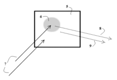
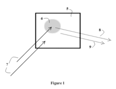
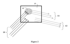
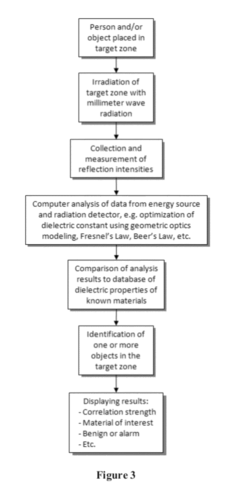
Method for identifying materials using dielectric properties through active millimeter wave illumination
PatentActiveUS8946641B2
Innovation
- An active millimeter wave imaging system that uses multiple frequencies between 5 and 500 GHz to measure the complex dielectric constant and optical properties of materials by analyzing the intensity of reflection from different illumination frequencies, comparing the data to a database to identify the composition of opaque materials.
Environmental Impact Assessment
The environmental impact assessment of magnesium nitride (Mg3N2) production and application is a critical aspect of its development as a dielectric material. The synthesis of Mg3N2 typically involves high-temperature reactions between magnesium and nitrogen gas, which can be energy-intensive and potentially contribute to greenhouse gas emissions if not managed properly. However, the overall environmental footprint of Mg3N2 production may be lower compared to some traditional dielectric materials, depending on the specific manufacturing processes employed.
In terms of resource consumption, magnesium is relatively abundant in the Earth's crust, which suggests a potentially sustainable supply chain for Mg3N2 production. The use of nitrogen gas in the synthesis process also presents minimal environmental concerns, as it is readily available from the atmosphere. However, the extraction and processing of magnesium from its ores may have localized environmental impacts, including land disturbance and water usage, which should be carefully managed.
The application of Mg3N2 as a dielectric material in electronic devices and components may offer environmental benefits through improved energy efficiency and device performance. Its unique dielectric properties could lead to the development of more compact and energy-efficient electronic systems, potentially reducing overall energy consumption and electronic waste. Additionally, the stability of Mg3N2 under various environmental conditions may contribute to longer-lasting devices, further reducing the environmental impact associated with electronic waste disposal.
However, the potential release of Mg3N2 into the environment during manufacturing, use, or disposal of electronic devices requires careful consideration. While magnesium nitride is generally considered non-toxic, its reactivity with water to form magnesium hydroxide and ammonia could have localized impacts on aquatic ecosystems if not properly managed. Proper handling, containment, and disposal protocols should be established to mitigate these risks.
The recyclability and end-of-life management of Mg3N2-containing devices also play a crucial role in its overall environmental impact. Research into efficient recycling methods for recovering and reprocessing Mg3N2 from electronic waste could significantly enhance its environmental profile. Furthermore, the development of closed-loop manufacturing processes and the implementation of extended producer responsibility programs could help minimize the environmental footprint of Mg3N2 throughout its lifecycle.
In conclusion, while the exploration of Mg3N2 as a dielectric material shows promise for enhancing electronic device performance, a comprehensive life cycle assessment is necessary to fully understand and optimize its environmental impact. This assessment should consider energy consumption, resource utilization, emissions, and waste management across all stages of Mg3N2 production, application, and disposal.
Mg3N2 Synthesis Techniques
The synthesis of magnesium nitride (Mg3N2) is a critical process in exploring its dielectric properties. Several techniques have been developed to produce high-quality Mg3N2 with controlled composition and morphology. One of the most common methods is direct nitridation, where magnesium metal is heated in a nitrogen atmosphere at temperatures ranging from 600°C to 1000°C. This process can be optimized by varying parameters such as temperature, pressure, and reaction time to achieve desired particle sizes and crystallinity.
Another effective technique is the ammonolysis of magnesium compounds. In this method, magnesium precursors such as magnesium oxide or magnesium hydroxide are treated with ammonia gas at elevated temperatures. This approach offers better control over the reaction conditions and can result in more uniform particle sizes compared to direct nitridation.
Plasma-enhanced chemical vapor deposition (PECVD) has emerged as a promising method for synthesizing Mg3N2 thin films. This technique involves the decomposition of magnesium-containing precursors in a nitrogen plasma environment. PECVD allows for the deposition of high-purity Mg3N2 films with excellent uniformity and controllable thickness, making it particularly suitable for electronic and optical applications.
Solution-based synthesis methods have also been developed for Mg3N2 production. These include solvothermal and hydrothermal processes, where magnesium precursors are reacted with nitrogen-containing compounds in sealed autoclaves under controlled temperature and pressure conditions. These methods often yield nanostructured Mg3N2 with unique morphologies, such as nanowires or nanoparticles, which can exhibit enhanced dielectric properties due to their high surface area.
Mechanochemical synthesis has gained attention as a solvent-free, environmentally friendly approach to Mg3N2 production. This technique involves the high-energy ball milling of magnesium powder in a nitrogen atmosphere, resulting in the formation of Mg3N2 through mechanical alloying and solid-state reactions. The mechanochemical method offers the advantage of producing nanocrystalline Mg3N2 at relatively low temperatures and without the need for complex equipment.
Recent advancements in synthesis techniques have focused on improving the purity and stoichiometry of Mg3N2. This includes the development of two-step synthesis processes, where an intermediate magnesium compound is first formed and then converted to Mg3N2 under controlled conditions. Such approaches have shown promise in reducing oxygen contamination and achieving better control over the final product's composition.
The choice of synthesis technique significantly influences the dielectric properties of the resulting Mg3N2. Factors such as particle size, crystallinity, and defect concentration can be tailored through careful selection and optimization of the synthesis method. As research in this field progresses, new and refined synthesis techniques are expected to emerge, further expanding the potential applications of Mg3N2 in dielectric and electronic devices.
Unlock deeper insights with Patsnap Eureka Quick Research — get a full tech report to explore trends and direct your research. Try now!
Generate Your Research Report Instantly with AI Agent
Supercharge your innovation with Patsnap Eureka AI Agent Platform!