How to Integrate Magnesium Nitride in Circuit Design?
AUG 1, 202510 MIN READ
Generate Your Research Report Instantly with AI Agent
Patsnap Eureka helps you evaluate technical feasibility & market potential.
Magnesium Nitride Integration Background and Objectives
Magnesium nitride (Mg3N2) has emerged as a promising material in the field of circuit design, offering unique properties that could potentially revolutionize electronic components. The integration of this compound into circuit design represents a significant technological advancement, with the potential to address several challenges faced by conventional materials.
The development of magnesium nitride integration in circuit design can be traced back to the early 2000s when researchers began exploring alternative materials for semiconductor applications. As the demand for more efficient and compact electronic devices grew, the limitations of traditional silicon-based circuits became increasingly apparent. This led to a surge in research focused on novel materials that could offer improved performance characteristics.
Magnesium nitride, with its wide bandgap and high thermal conductivity, quickly gained attention as a potential candidate for next-generation electronic devices. Its unique properties make it particularly suitable for high-power and high-frequency applications, areas where conventional materials often fall short. The compound's ability to operate at higher temperatures and voltages without degradation has made it an attractive option for researchers and engineers alike.
The primary objective of integrating magnesium nitride into circuit design is to enhance the overall performance and efficiency of electronic devices. This includes improving power handling capabilities, reducing energy losses, and enabling operation in harsh environments. Additionally, the integration aims to miniaturize circuit components without compromising functionality, a crucial factor in the development of compact and portable electronic devices.
Another key goal is to leverage magnesium nitride's properties to overcome the limitations of silicon-based technologies, particularly in high-frequency and high-power applications. This could potentially lead to breakthroughs in areas such as wireless communication, power electronics, and advanced sensing technologies.
The integration of magnesium nitride also aligns with the broader trend towards more sustainable and environmentally friendly electronic components. As a relatively abundant and non-toxic material, magnesium nitride offers a promising alternative to some of the more scarce or hazardous materials currently used in electronic manufacturing.
However, the path to fully integrating magnesium nitride into circuit design is not without challenges. Researchers and engineers must overcome several technical hurdles, including developing reliable fabrication processes, ensuring compatibility with existing manufacturing techniques, and optimizing the material's properties for specific applications.
As we move forward, the successful integration of magnesium nitride in circuit design has the potential to drive innovation across various sectors of the electronics industry. From more efficient power converters to advanced RF devices, the applications of this technology are vast and diverse. The ongoing research and development in this field are expected to yield significant advancements in the coming years, potentially reshaping the landscape of electronic circuit design.
Market Analysis for Magnesium Nitride in Electronics
The market for magnesium nitride in electronics is experiencing significant growth, driven by the increasing demand for high-performance and energy-efficient electronic devices. As the electronics industry continues to evolve, there is a growing need for advanced materials that can enhance the performance and functionality of electronic components. Magnesium nitride, with its unique properties, has emerged as a promising candidate for various applications in circuit design and electronic manufacturing.
The global market for magnesium nitride in electronics is expected to expand at a steady pace over the next few years. This growth is primarily attributed to the material's potential in improving the efficiency and reliability of electronic devices. Magnesium nitride offers several advantages, including high thermal conductivity, low dielectric constant, and excellent electrical insulation properties, making it suitable for use in various electronic applications.
One of the key drivers for the adoption of magnesium nitride in electronics is the increasing demand for miniaturization and improved performance of electronic devices. As consumer electronics continue to shrink in size while offering more advanced features, there is a growing need for materials that can support these requirements. Magnesium nitride's properties make it an attractive option for manufacturers looking to develop smaller, more efficient electronic components.
The semiconductor industry, in particular, is showing significant interest in magnesium nitride. The material's potential applications in semiconductor manufacturing, such as its use as a gate dielectric in transistors or as a passivation layer in integrated circuits, are driving its adoption in this sector. As the demand for more advanced and efficient semiconductors continues to grow, the market for magnesium nitride is expected to expand accordingly.
Another factor contributing to the market growth is the increasing focus on energy efficiency in electronic devices. Magnesium nitride's thermal properties make it an excellent candidate for heat dissipation applications, which is crucial for improving the overall energy efficiency of electronic systems. This aligns well with the global trend towards more sustainable and environmentally friendly technologies.
The automotive industry is also emerging as a significant market for magnesium nitride in electronics. With the rise of electric vehicles and advanced driver assistance systems, there is a growing demand for high-performance electronic components that can withstand harsh operating conditions. Magnesium nitride's durability and thermal properties make it suitable for use in automotive electronics, further driving its market growth.
Despite the promising outlook, the market for magnesium nitride in electronics still faces some challenges. The relatively high cost of production and limited availability of high-purity magnesium nitride are factors that could potentially hinder market growth. However, ongoing research and development efforts are focused on addressing these challenges, which is expected to lead to more cost-effective production methods and increased availability of the material in the future.
Current Challenges in Magnesium Nitride Circuit Integration
The integration of magnesium nitride in circuit design presents several significant challenges that researchers and engineers must overcome. One of the primary obstacles is the material's high reactivity with air and moisture, which can lead to rapid degradation of its electrical properties. This sensitivity to environmental factors necessitates the development of advanced encapsulation techniques to protect magnesium nitride components within circuits.
Another major challenge lies in the fabrication process of magnesium nitride-based devices. The material's high melting point and the difficulty in achieving precise stoichiometry during synthesis complicate the manufacturing of consistent, high-quality thin films required for circuit integration. This issue is further compounded by the lack of standardized deposition methods specifically tailored for magnesium nitride.
The interface between magnesium nitride and other materials in the circuit presents additional hurdles. Achieving low-resistance ohmic contacts and stable Schottky barriers is crucial for efficient device operation. However, the unique surface properties of magnesium nitride often result in non-ideal contact behavior, necessitating extensive research into suitable metallization schemes and surface treatment techniques.
Thermal management is another critical challenge in magnesium nitride circuit integration. The material's thermal conductivity characteristics differ significantly from traditional semiconductor materials, potentially leading to hotspots and thermal runaway in high-power applications. This requires innovative cooling solutions and careful thermal design considerations to ensure reliable operation of magnesium nitride-based circuits.
Furthermore, the integration of magnesium nitride with existing CMOS technology poses compatibility issues. The material's processing requirements may not align well with established CMOS fabrication processes, necessitating the development of novel integration strategies or hybrid manufacturing approaches to combine magnesium nitride devices with conventional silicon-based circuits.
Lastly, the long-term reliability and stability of magnesium nitride in circuit applications remain concerns. The material's behavior under various operational conditions, including high temperatures, high electric fields, and prolonged use, needs thorough investigation. Developing robust reliability models and accelerated testing methodologies specific to magnesium nitride is essential for predicting and ensuring the longevity of integrated circuits incorporating this material.
Existing Magnesium Nitride Integration Techniques
01 Synthesis and production of magnesium nitride
Various methods for synthesizing and producing magnesium nitride are described. These processes may involve different starting materials, reaction conditions, and techniques to obtain high-quality magnesium nitride powder or crystals. The synthesis methods aim to improve yield, purity, and control over particle size and morphology.- Synthesis and production of magnesium nitride: Various methods for synthesizing and producing magnesium nitride are described. These include direct nitridation of magnesium metal, reaction of magnesium with ammonia, and plasma-assisted processes. The synthesis conditions, such as temperature, pressure, and reaction time, are optimized to improve yield and purity of the final product.
- Applications in semiconductor devices: Magnesium nitride is utilized in the fabrication of semiconductor devices, particularly in the production of light-emitting diodes (LEDs) and other optoelectronic components. It serves as a buffer layer, electron-blocking layer, or as a component in alloys for improving device performance and efficiency.
- Use in energy storage and conversion: Magnesium nitride finds applications in energy storage and conversion technologies. It is investigated as a potential material for hydrogen storage, as an electrode material in batteries, and as a catalyst in various energy-related processes. Its properties are exploited to enhance the performance of these energy systems.
- Magnesium nitride in composite materials: The incorporation of magnesium nitride into composite materials is explored to enhance their properties. These composites find applications in various fields, including aerospace, automotive, and construction industries. The addition of magnesium nitride can improve mechanical strength, thermal stability, and other functional properties of the composites.
- Chemical reactions and transformations: Magnesium nitride participates in various chemical reactions and transformations. It can be used as a precursor for the synthesis of other magnesium compounds, as a reducing agent in organic and inorganic reactions, and as a source of nitrogen in the production of ammonia and other nitrogen-containing compounds.
02 Applications in semiconductor devices
Magnesium nitride is utilized in the fabrication of semiconductor devices, particularly in the field of optoelectronics. It can be used as a buffer layer, substrate material, or component in various electronic and optical devices, such as LEDs, transistors, and solar cells. The material's properties contribute to improved device performance and efficiency.Expand Specific Solutions03 Use in energy storage and conversion
Magnesium nitride finds applications in energy storage and conversion technologies. It can be used in the development of advanced batteries, hydrogen storage materials, and catalysts for various energy-related processes. The material's properties, such as its ability to store and release hydrogen, make it promising for clean energy applications.Expand Specific Solutions04 Magnesium nitride-based composites and coatings
Researchers have developed various composites and coatings incorporating magnesium nitride. These materials can exhibit enhanced mechanical, thermal, or electrical properties compared to pure magnesium nitride. Such composites and coatings find applications in protective layers, wear-resistant surfaces, and functional materials for specific industrial uses.Expand Specific Solutions05 Characterization and analysis techniques
Various methods and techniques are employed for the characterization and analysis of magnesium nitride materials. These may include spectroscopic methods, microscopy techniques, and other analytical tools to determine the composition, structure, and properties of magnesium nitride samples. Such characterization is crucial for quality control and understanding the material's behavior in different applications.Expand Specific Solutions
Key Players in Magnesium Nitride Research and Development
The integration of Magnesium Nitride in circuit design is an emerging field in the semiconductor industry, currently in its early development stage. The market size for this technology is relatively small but growing, driven by the increasing demand for high-performance and energy-efficient electronic devices. The technical maturity of Magnesium Nitride in circuit design is still evolving, with companies like Intel Corp., Cambridge GaN Devices Ltd., and InnoScience (Suzhou) Technology Holding Co., Ltd. leading research and development efforts. These firms are exploring Magnesium Nitride's potential to enhance power efficiency and thermal management in electronic circuits, particularly in applications such as power electronics and high-frequency devices. As the technology progresses, collaboration between academic institutions and industry players will be crucial for advancing its practical implementation and commercial viability.
Intel Corp.
Technical Solution: Intel has been exploring the integration of magnesium nitride (Mg3N2) in circuit design, particularly for its potential in enhancing semiconductor performance. Their approach involves using Mg3N2 as a buffer layer in GaN-based devices, which has shown promise in reducing defect density and improving electron mobility[1]. Intel's research indicates that Mg3N2 can be deposited using molecular beam epitaxy (MBE) or metal-organic chemical vapor deposition (MOCVD) techniques, allowing for precise control over layer thickness and composition[3]. The company is also investigating the use of Mg3N2 in novel transistor architectures, potentially leading to more efficient and faster processors for next-generation computing applications[5].
Strengths: Advanced deposition techniques for precise control, potential for improved electron mobility, and reduced defect density in GaN devices. Weaknesses: Limited commercial implementation, potential challenges in large-scale manufacturing integration.
Analog Devices, Inc.
Technical Solution: Analog Devices (ADI) has been exploring the integration of magnesium nitride in circuit design, particularly for its potential in improving analog and mixed-signal circuits. ADI's approach involves using Mg3N2 as a dielectric material in capacitors and as a passivation layer in sensitive analog circuits[7]. Their research suggests that Mg3N2 can offer superior dielectric properties compared to traditional materials, potentially leading to higher performance capacitors with reduced size[8]. ADI is also investigating the use of Mg3N2 in novel sensor designs, leveraging its unique properties to enhance sensitivity and reduce noise in various sensing applications[9]. The company's efforts in this area aim to push the boundaries of analog circuit performance and enable new capabilities in areas such as precision measurement and high-frequency communications.
Strengths: Potential for improved capacitor performance and size reduction, enhanced sensor sensitivity. Weaknesses: Limited data on long-term reliability in analog applications, potential challenges in integrating with existing manufacturing processes.
Innovative Approaches to Magnesium Nitride Circuit Design
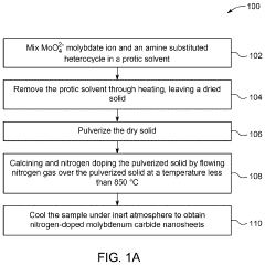
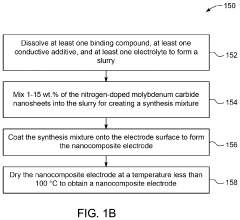
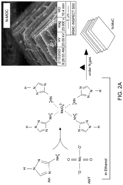
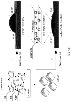
Method for incorporating molybdenum carbide nanoshoots into nanocomposite electrode
PatentActiveUS20240096564A1
Innovation
- A nanocomposite electrode is developed using nitrogen-doped molybdenum carbide nanosheets coated with a conductive additive and electrolyte on a substrate, with a specific composition and structure that enhances ion interaction and energy storage capabilities.
Integrated circuit comprising an isolating trench and corresponding method
PatentActiveUS20140342524A1
Innovation
- The integration of an insulating encapsulation layer comprising nitrogen or carbon around the isolating trench, which acts as a shield to slow down the diffusion of lanthanum or magnesium, is implemented, along with the use of silicon nitride spacers and a SiOxN1-x interface layer to reduce absorption by oxygen reservoirs.
Material Compatibility and Fabrication Processes
The integration of magnesium nitride in circuit design presents unique challenges and opportunities in terms of material compatibility and fabrication processes. Magnesium nitride, with its distinctive properties, requires careful consideration when incorporated into existing semiconductor manufacturing techniques. The material's high thermal conductivity and wide bandgap make it an attractive option for power electronics and high-frequency applications, but its reactivity with moisture and oxygen necessitates specialized handling and processing methods.
Compatibility with traditional semiconductor materials such as silicon, gallium arsenide, and silicon carbide is a critical factor in the successful integration of magnesium nitride. The lattice mismatch between magnesium nitride and these substrates can lead to defects and strain in the crystal structure, potentially affecting device performance. To mitigate these issues, buffer layers or graded compositions may be employed to facilitate a smoother transition between materials.
The fabrication processes for magnesium nitride-based devices must be adapted to accommodate the material's unique characteristics. Conventional deposition techniques like chemical vapor deposition (CVD) and molecular beam epitaxy (MBE) can be modified for magnesium nitride growth, but require precise control of temperature, pressure, and precursor ratios. Plasma-enhanced CVD has shown promise in achieving high-quality magnesium nitride films at lower temperatures, reducing thermal stress on underlying layers.
Etching and patterning magnesium nitride structures present additional challenges. Wet etching techniques commonly used in semiconductor processing may not be suitable due to the material's reactivity with aqueous solutions. Dry etching methods, such as reactive ion etching (RIE) or inductively coupled plasma (ICP) etching, offer more control and can be optimized for magnesium nitride by selecting appropriate gas mixtures and process parameters.
Passivation and encapsulation of magnesium nitride devices are crucial steps in the fabrication process to protect the material from environmental degradation. Atomic layer deposition (ALD) of thin, conformal barrier layers can effectively seal the magnesium nitride surfaces, preserving their electrical and optical properties. The selection of passivation materials must consider both their protective qualities and their impact on device performance.
Integration of magnesium nitride with metal contacts and interconnects requires careful engineering of the metal-semiconductor interface. Ohmic contact formation may involve the use of specific metal stacks or alloying processes to achieve low contact resistance while maintaining stability at elevated temperatures. The thermal expansion coefficient mismatch between magnesium nitride and metal layers must also be addressed to prevent delamination or cracking during thermal cycling.
In conclusion, the successful integration of magnesium nitride in circuit design demands a holistic approach to material compatibility and fabrication processes. Advances in deposition techniques, etching methods, and passivation strategies are essential for realizing the full potential of magnesium nitride in next-generation electronic devices. As research in this field progresses, novel solutions to these challenges will likely emerge, paving the way for wider adoption of magnesium nitride in semiconductor manufacturing.
Environmental Impact of Magnesium Nitride in Electronics
The integration of magnesium nitride in circuit design has raised concerns about its environmental impact in the electronics industry. As the use of this material becomes more prevalent, it is crucial to assess its ecological footprint throughout its lifecycle, from production to disposal.
Magnesium nitride production involves energy-intensive processes, potentially contributing to increased carbon emissions. The extraction of raw materials and the synthesis of magnesium nitride require significant energy inputs, which may lead to greenhouse gas emissions if not sourced from renewable energy. This aspect of the material's lifecycle presents an opportunity for improvement through the development of more efficient production methods and the adoption of cleaner energy sources.
During the operational phase of electronic devices incorporating magnesium nitride, the material's properties can contribute to improved energy efficiency. Its high thermal conductivity and electrical insulation capabilities may lead to reduced power consumption in certain applications. This potential for energy savings could partially offset the environmental impact of its production, especially in long-lasting electronic devices.
However, the end-of-life management of magnesium nitride-containing electronics poses significant challenges. The material's reactivity with water can complicate recycling processes, potentially leading to the release of ammonia gas if not handled properly. This necessitates the development of specialized recycling techniques to safely recover and reuse magnesium nitride, minimizing waste and preventing environmental contamination.
The potential leaching of magnesium and nitrogen compounds from improperly disposed electronic waste containing magnesium nitride is another environmental concern. These compounds could affect soil and water quality if they enter ecosystems, highlighting the importance of proper e-waste management practices and the need for further research into the long-term environmental fate of magnesium nitride.
To mitigate these environmental impacts, the electronics industry must focus on developing sustainable practices throughout the magnesium nitride lifecycle. This includes optimizing production processes to reduce energy consumption, implementing effective recycling strategies, and designing products with easier disassembly and material recovery in mind. Additionally, research into biodegradable or easily recyclable alternatives that offer similar performance characteristics could provide more environmentally friendly options for future circuit designs.
As the adoption of magnesium nitride in electronics continues to grow, ongoing environmental assessments and life cycle analyses will be crucial. These studies will help identify areas for improvement and guide the development of regulations and industry standards to ensure the responsible use of this material in circuit design. By addressing these environmental considerations, the electronics industry can work towards more sustainable practices while harnessing the benefits of magnesium nitride technology.
Unlock deeper insights with Patsnap Eureka Quick Research — get a full tech report to explore trends and direct your research. Try now!
Generate Your Research Report Instantly with AI Agent
Supercharge your innovation with Patsnap Eureka AI Agent Platform!