

How to Drive Innovations with PMMA Sputtering Techniques?
AUG 7, 20259 MIN READ
Generate Your Research Report Instantly with AI Agent
PatSnap Eureka helps you evaluate technical feasibility & market potential.
PMMA Sputtering Background
Poly(methyl methacrylate) (PMMA) sputtering is a cutting-edge technique in the field of thin film deposition, gaining significant attention in recent years due to its versatility and potential applications. This process involves the use of high-energy particles to eject PMMA molecules from a target material, which then condense onto a substrate to form a thin film. The technique has its roots in traditional sputtering methods used for metallic and inorganic materials, but has been adapted to accommodate the unique properties of PMMA.
The development of PMMA sputtering techniques can be traced back to the early 2000s when researchers began exploring ways to deposit organic materials using physical vapor deposition methods. Initially, the challenges were significant, as PMMA is a thermoplastic polymer with a relatively low melting point and is susceptible to degradation under high-energy bombardment. However, advancements in low-temperature plasma technologies and the development of specialized sputtering targets have made it possible to deposit PMMA films with controlled thickness and properties.
One of the key drivers behind the innovation in PMMA sputtering has been the growing demand for organic thin films in various industries. PMMA, known for its optical clarity, UV resistance, and biocompatibility, has found applications in fields such as optoelectronics, biomedical devices, and protective coatings. The ability to deposit PMMA films through sputtering offers several advantages over traditional solution-based methods, including better control over film thickness, improved adhesion to substrates, and the possibility of creating multilayer structures.
The evolution of PMMA sputtering techniques has been marked by several technological milestones. These include the development of magnetron sputtering systems optimized for organic materials, the introduction of pulsed DC sputtering to reduce thermal damage, and the use of reactive sputtering to modify the properties of deposited PMMA films. Additionally, researchers have explored co-sputtering techniques to create composite films combining PMMA with other materials, opening up new possibilities for tailored functional coatings.
As the field progresses, the focus of innovation in PMMA sputtering is shifting towards addressing specific challenges and expanding its applications. Current research efforts are aimed at improving the deposition rate, enhancing the uniformity of deposited films over large areas, and developing methods to control the molecular weight and cross-linking of PMMA during the sputtering process. These advancements are crucial for scaling up the technology for industrial applications and enabling the creation of more sophisticated PMMA-based devices and coatings.
Market Analysis for PMMA Coatings
The PMMA coatings market has witnessed significant growth in recent years, driven by the increasing demand for high-performance materials across various industries. PMMA, or polymethyl methacrylate, is a versatile thermoplastic known for its excellent optical clarity, weather resistance, and durability. These properties make PMMA coatings particularly attractive for applications in automotive, electronics, construction, and medical devices.
In the automotive sector, PMMA coatings are gaining traction for use in exterior and interior components, such as headlights, taillights, and display screens. The growing trend towards electric and autonomous vehicles is expected to further boost the demand for PMMA coatings in this industry. The electronics market is another key driver, with PMMA coatings being used in smartphones, tablets, and other consumer electronics to provide scratch resistance and enhanced durability.
The construction industry is also contributing to the growth of PMMA coatings, particularly in architectural applications. These coatings are used to protect building facades, windows, and decorative elements from environmental factors while maintaining aesthetic appeal. Additionally, the medical device sector is increasingly adopting PMMA coatings for their biocompatibility and resistance to sterilization processes.
Market research indicates that the global PMMA coatings market is projected to grow at a compound annual growth rate (CAGR) of over 6% from 2021 to 2026. This growth is attributed to the expanding end-use industries and the continuous development of innovative PMMA coating technologies, including sputtering techniques.
The Asia-Pacific region is expected to dominate the PMMA coatings market, driven by rapid industrialization, urbanization, and increasing disposable income in countries like China and India. North America and Europe are also significant markets, with a focus on high-value applications in aerospace and medical devices.
However, the market faces challenges such as volatile raw material prices and environmental concerns related to the production and disposal of PMMA coatings. This has led to increased research and development efforts to develop more sustainable and eco-friendly PMMA coating solutions, including bio-based alternatives and improved recycling technologies.
The competitive landscape of the PMMA coatings market is characterized by the presence of both large multinational corporations and smaller specialized companies. Key players are focusing on product innovation, strategic partnerships, and mergers and acquisitions to strengthen their market position and expand their product portfolios.
PMMA Sputtering Challenges
PMMA sputtering techniques face several significant challenges that hinder their widespread adoption and limit their potential for innovation. One of the primary obstacles is the low sputtering yield of PMMA compared to other materials. This low yield results in slower deposition rates, making the process less efficient and potentially more costly for large-scale production.
Another major challenge is the thermal sensitivity of PMMA. The material's low glass transition temperature makes it susceptible to thermal degradation during the sputtering process. This can lead to changes in the polymer's structure and properties, potentially compromising the quality and performance of the deposited films. Maintaining precise temperature control throughout the sputtering process is crucial but often difficult to achieve consistently.
The formation of uniform and defect-free PMMA films through sputtering is also a significant hurdle. PMMA tends to form irregular structures and exhibit poor adhesion to certain substrates, which can result in film delamination or non-uniform coverage. This issue is particularly problematic for applications requiring high-quality, conformal coatings.
Controlling the molecular weight and polydispersity of sputtered PMMA films presents another challenge. The sputtering process can cause polymer chain scission, leading to a reduction in molecular weight and changes in the material's properties. Achieving consistent molecular weight distribution across the deposited film is essential for maintaining uniform optical and mechanical properties.
The incorporation of functional groups or dopants into PMMA films during sputtering is also challenging. While this capability could greatly expand the potential applications of PMMA coatings, it requires precise control over the sputtering environment and target composition. Achieving homogeneous distribution of additives throughout the film remains a significant technical hurdle.
Scalability and reproducibility of PMMA sputtering processes pose additional challenges, particularly for industrial applications. Maintaining consistent film quality and properties across large substrate areas or in high-volume production settings requires sophisticated process control and monitoring systems.
Lastly, the environmental impact of PMMA sputtering processes is a growing concern. The use of organic solvents and potential generation of harmful byproducts during sputtering necessitate the development of more environmentally friendly approaches. Addressing these ecological considerations while maintaining process efficiency and film quality is a complex challenge that requires innovative solutions.
Current PMMA Sputtering Solutions
01 PMMA sputtering target preparation
Techniques for preparing PMMA sputtering targets, including methods for compressing PMMA powder, heat treatment processes, and surface finishing to create high-quality targets suitable for thin film deposition.- PMMA sputtering target preparation: Techniques for preparing PMMA sputtering targets, including methods for compressing PMMA powder, heat treatment processes, and surface finishing to create high-quality targets suitable for thin film deposition.
- Sputtering process optimization for PMMA films: Methods to optimize the sputtering process for PMMA, including adjusting power settings, gas flow rates, and substrate temperature to achieve desired film properties such as thickness uniformity and adhesion.
- PMMA-based composite sputtering targets: Development of composite sputtering targets incorporating PMMA with other materials to enhance specific properties of the deposited films, such as improved durability or optical characteristics.
- Surface modification of PMMA films by sputtering: Techniques for modifying the surface properties of PMMA films through sputtering, including the deposition of thin metal or oxide layers to enhance characteristics such as conductivity or hydrophobicity.
- PMMA sputtering for optical applications: Specialized sputtering techniques for PMMA in optical applications, focusing on achieving high transparency, controlled refractive index, and minimal light scattering for use in devices such as waveguides or optical coatings.
02 PMMA thin film deposition methods
Various sputtering techniques for depositing PMMA thin films, including RF magnetron sputtering, DC sputtering, and pulsed laser deposition. These methods focus on controlling film thickness, uniformity, and adhesion to different substrates.Expand Specific Solutions03 Surface modification of PMMA films
Techniques for modifying the surface properties of sputtered PMMA films, such as plasma treatment, ion bombardment, and chemical etching. These methods aim to enhance hydrophilicity, adhesion, or specific functional properties of the PMMA coating.Expand Specific Solutions04 PMMA-based composite coatings
Development of composite coatings using PMMA as a matrix material, incorporating nanoparticles, other polymers, or functional additives. These composite coatings are created through co-sputtering or layered deposition techniques to achieve enhanced properties.Expand Specific Solutions05 Characterization of sputtered PMMA films
Methods and techniques for analyzing and characterizing sputtered PMMA films, including thickness measurement, surface roughness analysis, chemical composition determination, and evaluation of optical and mechanical properties.Expand Specific Solutions
Key PMMA Sputtering Players
The PMMA sputtering techniques market is in a growth phase, driven by increasing demand in semiconductor, display, and optical industries. The market size is expanding, with projections indicating significant growth potential. Technologically, PMMA sputtering is advancing rapidly, with companies like Applied Materials, Canon Anelva, and ULVAC leading innovation. These firms, along with others such as Evatec and Soleras Advanced Coatings, are developing more efficient and precise sputtering systems. The technology's maturity varies across applications, with established processes in some sectors and emerging techniques in others. Collaboration between industry leaders and research institutions is accelerating technological progress and expanding potential applications.
Applied Materials, Inc.
Technical Solution: Applied Materials has developed advanced PMMA sputtering techniques for innovative applications in semiconductor and display manufacturing. Their PVD (Physical Vapor Deposition) systems utilize magnetron sputtering to deposit thin PMMA films with precise control over thickness and uniformity[1]. The company's Endura® platform incorporates multi-cathode PVD chambers capable of co-sputtering PMMA with other materials to create novel composite coatings[2]. Applied Materials has also pioneered the use of high-power impulse magnetron sputtering (HiPIMS) for PMMA deposition, which allows for denser films with improved adhesion and optical properties[3]. Their latest innovation involves the integration of in-situ plasma diagnostics and real-time process control to optimize PMMA sputtering parameters dynamically, resulting in enhanced film quality and reproducibility[4].
Strengths: Industry-leading PVD technology, extensive R&D capabilities, and a strong patent portfolio. Weaknesses: High equipment costs and complexity may limit adoption in some markets.
Soleras Advanced Coatings BV
Technical Solution: Soleras Advanced Coatings BV has focused on developing specialized PMMA sputtering techniques for high-performance coatings in various industries. Their rotatable magnetron sputtering technology has been adapted for PMMA deposition, allowing for high-rate, uniform coating of large-area substrates[16]. Soleras has introduced a novel plasma-enhanced sputtering process that improves the cross-linking of PMMA during deposition, resulting in coatings with enhanced chemical resistance and durability[17]. The company has also developed a unique target design that optimizes PMMA utilization and reduces particle generation during sputtering, leading to improved film quality and cost-effectiveness[18]. Additionally, Soleras has pioneered the use of cylindrical magnetron sputtering for PMMA, which enables conformal coating of complex 3D structures for advanced applications in optics and microelectronics[19].
Strengths: Expertise in rotatable magnetron technology, specialized target designs, focus on large-area coatings. Weaknesses: More limited product range compared to full-service equipment manufacturers.
PMMA Sputtering Innovations
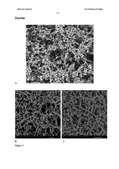
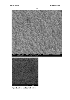
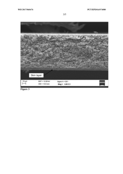
A method for the production of poly(methyl methacrylate) (PMMA) membranes and uses thereof
PatentInactiveEP3359285A1
Innovation
- A method for producing highly porous, symmetric reticulated PMMA membranes using a thin film casting and solvent removal process, combined with hydrophilization techniques, to create a composite membrane with enhanced capillary flow and protein binding capacity, overcoming the limitations of previous PMMA membrane production methods.
A method for the production of poly(methyl methacrylate) (PMMA) membranes and uses thereof
PatentWO2017060476A1
Innovation
- A method for producing highly porous, symmetric reticulated PMMA membranes using a thin film casting and solvent removal process, coupled with hydrophilization techniques, to enhance capillary flow and protein binding capacity, using a suitable support material like polyester to improve durability.
PMMA Sputtering Applications
PMMA sputtering techniques have found a wide range of applications across various industries, driving innovation in multiple fields. In the semiconductor industry, PMMA sputtering is utilized for creating high-resolution photoresist patterns in lithography processes. This application enables the fabrication of increasingly smaller and more complex integrated circuits, pushing the boundaries of Moore's Law and advancing the capabilities of electronic devices.
In the optical industry, PMMA sputtering plays a crucial role in the production of anti-reflective coatings for lenses and other optical components. By depositing thin layers of PMMA onto glass or plastic surfaces, manufacturers can significantly reduce light reflection and improve the overall performance of optical systems. This technology has led to advancements in camera lenses, eyeglasses, and display screens, enhancing image quality and reducing glare.
The biomedical field has also benefited from PMMA sputtering applications. Researchers have employed this technique to create biocompatible coatings for medical implants and devices. These coatings can improve the integration of implants with surrounding tissues, reduce the risk of rejection, and enhance the overall performance of medical devices. Additionally, PMMA sputtering has been used to develop biosensors and lab-on-a-chip devices, enabling more efficient and accurate diagnostic tools.
In the field of energy storage, PMMA sputtering has shown promise in the development of advanced battery technologies. By applying PMMA coatings to electrode materials, researchers have been able to improve the stability and performance of lithium-ion batteries. This application has the potential to enhance the energy density and lifespan of batteries, contributing to the advancement of electric vehicles and renewable energy storage systems.
The aerospace industry has also embraced PMMA sputtering techniques for various applications. One notable use is in the development of protective coatings for aircraft components. These coatings can improve resistance to wear, corrosion, and environmental factors, ultimately extending the lifespan of critical aerospace parts. Furthermore, PMMA sputtering has been employed in the creation of specialized optical coatings for spacecraft windows and sensors, enhancing their performance in extreme space environments.
In the field of nanotechnology, PMMA sputtering has enabled the fabrication of nanostructures and devices with unprecedented precision. Researchers have utilized this technique to create nanoscale patterns and templates for the development of novel materials and devices. This application has opened up new possibilities in areas such as nanoelectronics, photonics, and quantum computing, driving innovation at the smallest scales.
Environmental Impact of PMMA Sputtering
PMMA sputtering techniques, while innovative and effective for various applications, have potential environmental impacts that warrant careful consideration. The process involves the use of energy-intensive equipment and materials that may contribute to greenhouse gas emissions. The sputtering process itself can release particulate matter and volatile organic compounds (VOCs) into the atmosphere, which may have localized air quality impacts if not properly controlled.
The production and disposal of PMMA targets used in sputtering also present environmental challenges. PMMA is a thermoplastic derived from petrochemicals, and its production involves energy-intensive processes and potential chemical emissions. While PMMA is recyclable, the specialized nature of sputtering targets may limit recycling options, potentially leading to increased waste generation.
Water usage and potential contamination are additional environmental concerns associated with PMMA sputtering. The process may require cooling systems or cleaning procedures that consume water resources. Wastewater from these processes may contain trace amounts of PMMA particles or other chemicals used in the sputtering process, necessitating proper treatment before discharge.
The use of inert gases, such as argon, in PMMA sputtering processes also has environmental implications. While these gases are not directly harmful to the environment, their production, transportation, and storage contribute to the overall carbon footprint of the technology. Additionally, any leaks or improper handling of these gases can lead to unnecessary emissions.
To mitigate these environmental impacts, researchers and industry practitioners are exploring several avenues for improvement. These include developing more energy-efficient sputtering equipment, implementing closed-loop recycling systems for PMMA targets, and optimizing process parameters to reduce waste and emissions. Some facilities are also investigating the use of renewable energy sources to power sputtering equipment, further reducing the carbon footprint of the technology.
Advancements in PMMA formulations and target designs are also being pursued to enhance the environmental profile of sputtering techniques. These innovations aim to improve the recyclability of targets, reduce the amount of material needed for effective sputtering, and minimize the generation of particulate matter during the process.
As the technology continues to evolve, it is crucial for stakeholders to prioritize environmental considerations alongside performance and cost factors. This holistic approach will be essential for driving sustainable innovations in PMMA sputtering techniques and ensuring their long-term viability in various industrial applications.
Unlock deeper insights with PatSnap Eureka Quick Research — get a full tech report to explore trends and direct your research. Try now!
Generate Your Research Report Instantly with AI Agent
Supercharge your innovation with PatSnap Eureka AI Agent Platform!