Impact of photodiode material purity on detection fidelity
AUG 21, 202510 MIN READ
Generate Your Research Report Instantly with AI Agent
Patsnap Eureka helps you evaluate technical feasibility & market potential.
Photodiode Purity and Detection Fidelity: Background and Objectives
Photodiodes have been at the forefront of light detection technology for decades, playing a crucial role in various applications ranging from telecommunications to medical imaging. The evolution of photodiode technology has been closely tied to advancements in material science and semiconductor fabrication techniques. As the demand for higher performance and more sensitive light detection systems continues to grow, the impact of photodiode material purity on detection fidelity has become a critical area of focus for researchers and industry professionals alike.
The primary objective of this technical research report is to comprehensively examine the relationship between photodiode material purity and detection fidelity. By exploring this connection, we aim to identify potential avenues for improving photodiode performance and reliability across a wide range of applications. This investigation is particularly timely given the increasing importance of high-fidelity light detection in emerging fields such as quantum computing, lidar systems for autonomous vehicles, and ultra-sensitive scientific instrumentation.
To fully understand the significance of material purity in photodiode performance, it is essential to trace the historical development of photodiode technology. Early photodiodes were primarily constructed using silicon, which remains a popular material choice due to its abundance and well-established manufacturing processes. However, as applications demanded greater sensitivity and broader spectral responses, researchers began exploring alternative materials such as germanium, indium gallium arsenide, and various III-V compound semiconductors.
The pursuit of higher purity materials has been driven by the recognition that impurities and defects in the semiconductor lattice can significantly impact a photodiode's performance. These imperfections can act as recombination centers, trapping charge carriers and reducing the device's quantum efficiency. Additionally, impurities can contribute to dark current, a source of noise that limits the photodiode's ability to detect weak signals. As a result, the development of ultra-high purity materials and advanced purification techniques has become a key focus in the field of photodiode research and development.
In recent years, the emergence of new applications has further emphasized the need for photodiodes with exceptional detection fidelity. For instance, the growing field of quantum information processing requires single-photon detectors with near-perfect efficiency and minimal noise. Similarly, advanced spectroscopy techniques and high-speed optical communication systems demand photodiodes with rapid response times and low dark current. These applications have pushed the boundaries of what is possible with current photodiode technology, highlighting the critical role that material purity plays in achieving the desired performance characteristics.
As we delve deeper into this technical research report, we will explore the current state of photodiode material purity, the challenges faced in achieving higher levels of purity, and the potential impact of these advancements on detection fidelity. By examining these aspects, we aim to provide valuable insights that can guide future research and development efforts in the field of photodiode technology.
Market Demand for High-Fidelity Photodetectors
The market demand for high-fidelity photodetectors has been steadily increasing across various industries, driven by the growing need for precise light detection and measurement in applications ranging from scientific research to advanced manufacturing. The global photodetector market is experiencing significant growth, with a particular emphasis on high-performance devices that can deliver superior detection fidelity.
In the telecommunications sector, the rollout of 5G networks and the ongoing development of fiber-optic communication systems have created a surge in demand for high-fidelity photodetectors. These devices are crucial for ensuring reliable and high-speed data transmission over long distances. The increasing data traffic and the need for faster, more efficient communication networks continue to fuel the market for advanced photodetectors.
The healthcare and life sciences industries represent another major market for high-fidelity photodetectors. Applications such as flow cytometry, DNA sequencing, and medical imaging require extremely sensitive and accurate light detection capabilities. As personalized medicine and advanced diagnostic techniques gain traction, the demand for photodetectors with enhanced material purity and detection fidelity is expected to rise significantly.
In the automotive industry, the development of advanced driver-assistance systems (ADAS) and autonomous vehicles has created a new market segment for high-performance photodetectors. These sensors are essential for LiDAR systems, which require precise light detection for accurate distance measurement and object recognition. The growing adoption of electric vehicles and the push towards higher levels of vehicle autonomy are driving the demand for more sophisticated photodetector technologies.
The aerospace and defense sectors also contribute significantly to the market demand for high-fidelity photodetectors. Applications such as satellite communications, remote sensing, and target acquisition systems rely heavily on advanced photodetection technologies. The increasing focus on space exploration and Earth observation missions further amplifies the need for photodetectors with exceptional performance characteristics.
Environmental monitoring and climate research represent emerging markets for high-fidelity photodetectors. These devices play a crucial role in atmospheric studies, pollution monitoring, and spectroscopic analysis of various environmental phenomena. As global efforts to combat climate change intensify, the demand for more accurate and sensitive photodetection systems is expected to grow.
The industrial sector, particularly in areas such as process control, quality assurance, and machine vision, is another significant driver of market demand for high-fidelity photodetectors. The ongoing trend towards Industry 4.0 and smart manufacturing has increased the need for precise sensing technologies, including advanced photodetectors, to enable real-time monitoring and control of production processes.
As the market for high-fidelity photodetectors continues to expand, there is a growing emphasis on improving material purity to enhance detection fidelity. This trend is likely to drive further innovation in photodiode materials and manufacturing processes, ultimately leading to the development of more sensitive, reliable, and efficient photodetection systems across various industries.
Current Challenges in Photodiode Material Purity
The current challenges in photodiode material purity are multifaceted and significantly impact the detection fidelity of these crucial optoelectronic devices. One of the primary issues is the presence of impurities and defects in the semiconductor materials used to fabricate photodiodes. These impurities can act as trapping centers for charge carriers, leading to increased dark current and reduced sensitivity.
Crystal growth techniques, such as Czochralski and float-zone methods, have made substantial progress in producing high-purity silicon and germanium. However, achieving ultra-high purity levels consistently remains a challenge, especially for compound semiconductors like gallium arsenide and indium gallium arsenide. The presence of even trace amounts of impurities can dramatically alter the electrical and optical properties of these materials.
Another significant challenge is the control of dopant concentrations and distributions within the photodiode structure. Precise doping is critical for optimizing the depletion region and minimizing parasitic capacitance. However, achieving uniform doping profiles across large wafers and maintaining consistency between production batches is technically demanding and often leads to variations in device performance.
Surface contamination and interface states pose additional challenges to material purity. Even if the bulk material is of high purity, surface defects and impurities can dominate device performance, particularly in thin-film and nanostructured photodiodes. These surface states can lead to increased recombination rates and reduced quantum efficiency.
The purity requirements for photodiode materials become even more stringent as devices are scaled down and integrated into complex optoelectronic systems. Nanoscale impurities and structural defects that were previously negligible can now significantly impact device performance. This scaling challenge is particularly evident in the development of avalanche photodiodes and single-photon detectors, where material purity directly affects noise characteristics and detection efficiency.
Environmental factors during manufacturing and packaging also present challenges to maintaining material purity. Contamination from processing equipment, clean room environments, and packaging materials can introduce impurities that are difficult to eliminate. Additionally, the high-temperature processes often used in device fabrication can cause the redistribution of impurities and the generation of new defects.
Addressing these challenges requires advancements in material science, fabrication technologies, and characterization techniques. Innovations in purification methods, such as zone refining and chemical vapor deposition, are needed to push the boundaries of material purity. Furthermore, the development of more sensitive analytical tools for detecting and quantifying impurities at ever-lower concentrations is crucial for continued progress in this field.
Existing Solutions for Enhancing Material Purity
01 Improved photodiode structure for enhanced detection fidelity
Advanced photodiode designs incorporate structural improvements to enhance detection fidelity. These may include optimized doping profiles, novel junction configurations, or the integration of light-trapping features. Such enhancements can lead to increased sensitivity, reduced noise, and improved overall performance in various sensing applications.- Improved photodiode structure for enhanced detection fidelity: Advanced photodiode designs incorporate structural improvements to enhance detection fidelity. These may include optimized doping profiles, novel junction configurations, or the integration of light-trapping features. Such enhancements can lead to increased sensitivity, reduced noise, and improved overall performance in various sensing applications.
- Signal processing techniques for photodiode output: Various signal processing methods are employed to improve the fidelity of photodiode detection. These techniques may include noise reduction algorithms, adaptive filtering, or advanced amplification circuits. By implementing these methods, the signal-to-noise ratio can be significantly improved, leading to more accurate and reliable photodiode measurements.
- Integration of photodiodes with readout circuits: The integration of photodiodes with specialized readout circuits can greatly enhance detection fidelity. These circuits may include charge-coupled devices (CCDs), CMOS image sensors, or custom-designed analog-to-digital converters. Such integration allows for optimized signal acquisition and processing, resulting in improved overall system performance.
- Temperature compensation and stabilization techniques: Various methods are employed to compensate for temperature-induced variations in photodiode performance. These may include the use of temperature sensors, feedback control systems, or materials with low temperature coefficients. By minimizing the effects of temperature fluctuations, the detection fidelity of photodiodes can be maintained across a wide range of operating conditions.
- Optical enhancements for improved photodiode sensitivity: Optical techniques are utilized to enhance the sensitivity and fidelity of photodiode detection. These may include the use of anti-reflective coatings, microlens arrays, or waveguide structures. By optimizing the optical path and increasing light collection efficiency, these enhancements can significantly improve the overall performance of photodiode-based sensing systems.
02 Signal processing techniques for photodiode output
Various signal processing methods are employed to improve the fidelity of photodiode detection. These techniques may include noise reduction algorithms, adaptive filtering, or advanced amplification circuits. By implementing these processing strategies, the signal-to-noise ratio can be significantly improved, leading to more accurate and reliable photodiode measurements.Expand Specific Solutions03 Temperature compensation in photodiode detection
Temperature fluctuations can affect photodiode performance and detection fidelity. Implementing temperature compensation techniques, such as integrated temperature sensors or adaptive biasing circuits, can mitigate these effects. This approach ensures consistent and accurate photodiode response across a wide range of operating temperatures.Expand Specific Solutions04 Integration of photodiodes with advanced readout circuits
Combining photodiodes with sophisticated readout integrated circuits (ROICs) can significantly enhance detection fidelity. These integrated systems may incorporate on-chip analog-to-digital converters, programmable gain amplifiers, or digital signal processing units. Such integration allows for real-time signal optimization and improved overall system performance.Expand Specific Solutions05 Novel materials and fabrication techniques for high-fidelity photodiodes
Exploring new materials and innovative fabrication methods can lead to photodiodes with superior detection fidelity. This may include the use of III-V semiconductors, nanostructured materials, or advanced epitaxial growth techniques. These approaches can result in photodiodes with enhanced quantum efficiency, lower dark current, and improved spectral response.Expand Specific Solutions
Key Players in Photodiode Manufacturing Industry
The photodiode material purity detection fidelity market is in a growth phase, driven by increasing demand for high-performance sensors across industries. The global market size is expanding, with key players like Sony Semiconductor Solutions, Hamamatsu Photonics, and Sharp Corp leading innovation. Technological maturity varies, with established companies like Samsung Display and BOE Technology Group focusing on advanced materials and manufacturing processes. Emerging players such as X-FAB Global Services and Varex Imaging are contributing to market diversification. Overall, the industry is characterized by ongoing research and development efforts to improve material purity and detection accuracy, with a trend towards specialized applications in automotive, medical, and industrial sectors.
Sony Semiconductor Solutions Corp.
Technical Solution: Sony Semiconductor Solutions has pioneered the development of stacked CMOS image sensors with backside illumination technology. Their approach to improving photodiode material purity involves a unique combination of wafer bonding and thinning processes[2]. This allows for the separation of the photodiode layer from the readout circuitry, enabling the use of highly optimized, ultra-pure silicon for the photosensitive region. Sony has also implemented advanced gettering techniques to remove impurities from the active regions of their photodiodes[4]. Additionally, they have developed proprietary doping profiles that minimize lattice defects and enhance charge collection efficiency[6]. These innovations have resulted in image sensors with significantly improved low-light performance and reduced noise levels.
Strengths: High sensitivity and low noise due to optimized photodiode purity; excellent performance in low-light conditions. Weaknesses: Complex manufacturing process; potentially higher costs compared to conventional sensors.
Hamamatsu Photonics KK
Technical Solution: Hamamatsu Photonics has developed advanced photodiode technologies focusing on high-purity silicon and compound semiconductor materials. Their approach involves ultra-high purification processes for silicon, achieving impurity concentrations below 1 part per trillion[1]. This results in photodiodes with extremely low dark current and high quantum efficiency. They have also implemented novel crystal growth techniques for compound semiconductors like InGaAs, allowing for precise control of material composition and defect density[3]. These advancements have led to photodiodes with enhanced spectral response and improved detection fidelity across a wide range of wavelengths, from ultraviolet to near-infrared[5].
Strengths: Exceptional material purity leading to superior detection fidelity; wide spectral range coverage. Weaknesses: Higher production costs; complexity in manufacturing processes.
Innovations in High-Purity Photodiode Materials
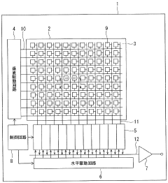
Photodiode with a reduced dark current and method for the production thereof
PatentInactiveEP1891682A1
Innovation
- A diode design where the pn junction is formed between a doping region of the first conductivity type on a crystalline substrate and a second semiconductor layer, with additional doping at the edge of the doped region to move the pn junction deeper into the substrate, thereby isolating imperfections from the space charge zone, and using a thin, highly doped first semiconductor layer to minimize dark current.
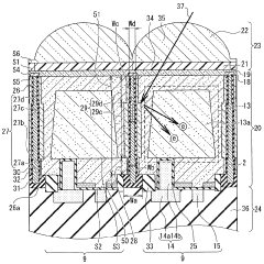
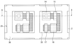
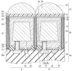
Light detection device and electronic device
PatentWO2023157496A1
Innovation
- A photodetector design with a substrate featuring trench portions of varying widths and semiconductor regions of opposite conductivity type, where the impurity concentration is lower on the side opposite to the light-receiving surface and higher on the light-receiving surface, to optimize impurity distribution and reduce electric fields in pixel transistors.
Environmental Impact of Photodiode Manufacturing Processes
The manufacturing processes of photodiodes have significant environmental implications, particularly concerning material purity and its impact on detection fidelity. The production of high-purity semiconductor materials, essential for photodiode fabrication, involves energy-intensive processes and potentially hazardous chemicals, raising environmental concerns.
Semiconductor purification, a critical step in photodiode manufacturing, often requires extensive energy consumption and generates substantial waste. The Czochralski process, commonly used for silicon crystal growth, demands high temperatures and prolonged heating periods, resulting in considerable energy expenditure and associated carbon emissions. Moreover, the process generates silicon tetrachloride as a by-product, which can be harmful if not properly managed.
Chemical vapor deposition (CVD), another crucial technique in photodiode production, utilizes various precursor gases that may contribute to air pollution if not adequately controlled. Some of these gases, such as silane and phosphine, are highly toxic and require stringent safety measures during handling and disposal.
Water usage in semiconductor manufacturing is another environmental concern. The production of ultra-pure water, necessary for cleaning and processing, consumes substantial amounts of water and energy. Additionally, the resulting wastewater often contains trace amounts of chemicals and metals, requiring extensive treatment before release.
The etching processes used in photodiode fabrication typically involve strong acids or plasma, which can generate hazardous waste. Proper disposal and treatment of these materials are essential to prevent soil and water contamination. Furthermore, the use of rare earth elements in some specialized photodiodes raises concerns about resource depletion and the environmental impact of mining operations.
Efforts to mitigate these environmental impacts are ongoing within the industry. Recycling and reclamation of materials, particularly silicon and precious metals, have become increasingly common. Advanced effluent treatment systems are being implemented to reduce water consumption and improve wastewater quality. Some manufacturers are also exploring alternative production methods, such as epitaxial growth techniques, which may offer reduced environmental footprints compared to traditional bulk crystal growth.
The push for higher material purity to enhance detection fidelity presents a challenge in balancing performance improvements with environmental sustainability. As the demand for more sensitive photodiodes grows, particularly in emerging applications like quantum computing and advanced medical imaging, the industry must innovate to develop cleaner, more efficient manufacturing processes that maintain the required level of material purity while minimizing environmental impact.
Standardization and Quality Control in Photodiode Production
Standardization and quality control in photodiode production play a crucial role in ensuring the consistency and reliability of photodiode performance, particularly in relation to material purity and its impact on detection fidelity. The implementation of rigorous standards and quality control measures throughout the production process is essential to maintain high-quality outputs and meet the demanding requirements of various applications.
One of the primary focuses of standardization in photodiode production is the establishment of precise specifications for material purity. This includes defining acceptable levels of impurities and defects in the semiconductor materials used, such as silicon or germanium. These standards are typically based on extensive research and industry best practices, taking into account the specific requirements of different photodiode types and applications.
Quality control measures in photodiode production often involve a combination of in-process and final product testing. In-process testing may include regular checks of material purity during various stages of production, such as wafer fabrication and doping processes. This allows for early detection of any deviations from the established standards and enables prompt corrective actions to be taken.
Final product testing is equally critical in ensuring that the produced photodiodes meet the required specifications for detection fidelity. This typically involves a series of electrical and optical tests to verify parameters such as responsivity, dark current, and spectral response. Advanced testing equipment and methodologies are employed to accurately measure these characteristics and ensure compliance with the established standards.
The implementation of statistical process control (SPC) techniques is another important aspect of quality control in photodiode production. SPC involves the continuous monitoring of production processes using statistical methods to identify and reduce variability. This approach helps maintain consistent material purity levels and overall product quality across production batches.
Traceability is a key component of effective quality control in photodiode manufacturing. This involves maintaining detailed records of material sources, production processes, and test results for each batch of photodiodes. Such documentation not only aids in troubleshooting and process improvement but also provides valuable data for ongoing research and development efforts aimed at enhancing photodiode performance and material purity.
Collaboration between manufacturers, research institutions, and industry bodies is essential for the development and refinement of standardization and quality control practices. This collaborative approach ensures that standards evolve in line with technological advancements and changing market requirements, ultimately contributing to the continuous improvement of photodiode performance and reliability.
Unlock deeper insights with Patsnap Eureka Quick Research — get a full tech report to explore trends and direct your research. Try now!
Generate Your Research Report Instantly with AI Agent
Supercharge your innovation with Patsnap Eureka AI Agent Platform!