Optimizing photodiode functionalities for microscopy techniques
AUG 21, 20259 MIN READ
Generate Your Research Report Instantly with AI Agent
Patsnap Eureka helps you evaluate technical feasibility & market potential.
Photodiode Microscopy Evolution and Objectives
Photodiode technology has undergone significant evolution in the field of microscopy, transforming the capabilities and applications of various imaging techniques. The journey began with simple light-sensitive devices and has progressed to highly sophisticated, multi-functional photodiodes that play a crucial role in modern microscopy systems.
In the early stages, photodiodes were primarily used as basic light detectors in microscopes, providing rudimentary light intensity measurements. As technology advanced, researchers and engineers recognized the potential for photodiodes to enhance microscopy techniques beyond simple light detection. This realization led to a series of innovations aimed at optimizing photodiode functionalities specifically for microscopy applications.
One of the key developments in this evolution was the improvement of photodiode sensitivity and response time. Enhanced sensitivity allowed for the detection of extremely low light levels, enabling the observation of faint specimens and fluorescent markers. Faster response times made it possible to capture rapid biological processes and dynamic events at the cellular level.
The integration of photodiodes with advanced readout electronics marked another significant milestone. This integration facilitated precise quantification of light signals, enabling more accurate and reproducible measurements in microscopy experiments. It also paved the way for the development of high-resolution imaging techniques, such as confocal microscopy and super-resolution microscopy.
As the field progressed, researchers focused on expanding the spectral range of photodiodes. This expansion allowed for the detection of a wider range of wavelengths, from ultraviolet to near-infrared, opening up new possibilities for multi-color imaging and spectroscopic analysis in microscopy. The ability to simultaneously detect multiple wavelengths led to the development of advanced fluorescence microscopy techniques, enabling the study of complex cellular interactions and molecular processes.
The miniaturization of photodiodes has been another crucial aspect of their evolution in microscopy. Smaller, more efficient photodiodes have enabled the design of compact microscopy systems with improved spatial resolution. This miniaturization has also facilitated the integration of multiple photodiodes into array formats, allowing for parallel detection and imaging of larger sample areas.
Looking ahead, the objectives for further optimizing photodiode functionalities in microscopy are multifaceted. Researchers aim to push the boundaries of sensitivity, striving to detect single-photon events reliably. This would enable unprecedented levels of detection in low-light conditions and open up new avenues for studying extremely faint biological samples.
Another key objective is to improve the temporal resolution of photodiode-based detection systems. Achieving faster response times and higher frame rates would allow for the capture of rapid biological processes with greater precision, advancing our understanding of dynamic cellular events.
Market Analysis for Advanced Microscopy Solutions
The advanced microscopy solutions market is experiencing significant growth, driven by increasing demand for high-resolution imaging in various scientific and industrial applications. This market segment encompasses a wide range of technologies, including confocal microscopy, super-resolution microscopy, and multiphoton microscopy, all of which rely heavily on optimized photodiode functionalities.
The global market for advanced microscopy solutions is projected to expand at a compound annual growth rate (CAGR) of 8.5% from 2021 to 2026. This growth is primarily fueled by advancements in life sciences research, materials science, and nanotechnology. The increasing focus on precision medicine and personalized healthcare has also contributed to the rising demand for sophisticated imaging techniques.
In the life sciences sector, there is a growing need for advanced microscopy solutions in fields such as cell biology, neuroscience, and developmental biology. These applications require high-sensitivity photodiodes capable of detecting low-light signals and minimizing noise, which are crucial for studying cellular processes and molecular interactions at the nanoscale level.
The materials science and semiconductor industries are also driving market growth, as they require advanced microscopy techniques for quality control, failure analysis, and research and development. In these sectors, photodiodes with enhanced spectral response and improved quantum efficiency are essential for achieving accurate and detailed imaging results.
Geographically, North America and Europe currently dominate the advanced microscopy solutions market, accounting for over 60% of the global market share. However, the Asia-Pacific region is expected to witness the fastest growth in the coming years, driven by increasing research and development activities in countries like China, Japan, and South Korea.
Key players in the advanced microscopy solutions market include established companies such as Carl Zeiss, Nikon, Olympus, and Leica Microsystems, as well as emerging players focusing on innovative technologies. These companies are investing heavily in research and development to improve photodiode functionalities and integrate them into their microscopy systems.
The market is also seeing a trend towards the development of integrated microscopy platforms that combine multiple imaging modalities. This integration requires photodiodes with enhanced versatility and adaptability to different imaging techniques, presenting both challenges and opportunities for manufacturers.
As the demand for higher resolution and more sensitive imaging continues to grow, the optimization of photodiode functionalities remains a critical factor in the advancement of microscopy techniques. This presents significant opportunities for companies specializing in photodiode technology to collaborate with microscope manufacturers and research institutions to develop next-generation imaging solutions.
Current Photodiode Limitations in Microscopy
Photodiodes play a crucial role in microscopy techniques, serving as essential components for light detection and image formation. However, current photodiode technologies face several limitations that hinder their optimal performance in advanced microscopy applications. One of the primary challenges is the trade-off between sensitivity and speed. High-sensitivity photodiodes often suffer from slower response times, limiting their ability to capture rapid dynamic processes in live-cell imaging or high-speed confocal microscopy.
Another significant limitation is the limited dynamic range of conventional photodiodes. This constraint makes it difficult to accurately detect both weak and strong signals simultaneously, which is particularly problematic in fluorescence microscopy where signal intensities can vary greatly across different samples or within a single field of view. The inability to capture the full range of light intensities can lead to loss of valuable information in both bright and dim regions of the specimen.
Noise is another critical factor affecting photodiode performance in microscopy. Dark current noise, shot noise, and thermal noise can all contribute to reduced signal-to-noise ratios, especially when dealing with low-light conditions or weak fluorescence signals. This noise limitation becomes particularly apparent in techniques such as single-molecule imaging or super-resolution microscopy, where the detection of individual photons is crucial.
The spectral response of photodiodes also presents challenges in microscopy applications. Many conventional photodiodes have limited sensitivity in certain wavelength ranges, particularly in the near-infrared and ultraviolet regions. This spectral limitation can restrict the types of fluorophores or contrast agents that can be effectively detected, potentially limiting the scope of microscopy experiments.
Size and integration issues also pose challenges for photodiode implementation in microscopy systems. Miniaturization of photodiodes while maintaining high performance is essential for developing compact and high-resolution microscopy instruments. However, reducing the size of photodiodes often comes at the cost of decreased sensitivity or increased noise, creating a design challenge for microscope manufacturers.
Lastly, the uniformity and reproducibility of photodiode arrays used in imaging applications can be problematic. Variations in sensitivity and response across different pixels in an array can lead to image artifacts and non-uniform detection, affecting the overall quality and reliability of microscopy data. Addressing these limitations is crucial for advancing the capabilities of microscopy techniques and enabling new discoveries in fields such as cell biology, neuroscience, and materials science.
Existing Photodiode Optimization Techniques
01 Light detection and conversion
Photodiodes are primarily used for detecting light and converting it into electrical signals. They can be used in various applications such as optical communication systems, image sensors, and light measurement devices. The efficiency and sensitivity of photodiodes can be enhanced through different structural designs and materials.- Light detection and conversion: Photodiodes are primarily used for detecting light and converting it into electrical signals. They can be used in various applications such as optical communication, image sensors, and light measurement devices. The efficiency and sensitivity of photodiodes can be enhanced through different structural designs and materials.
- Integration with other electronic components: Photodiodes can be integrated with other electronic components to create more complex systems. This integration can include combining photodiodes with amplifiers, transistors, or other sensors to enhance functionality and performance. Such integrated systems can be used in applications like optical transceivers, smart lighting systems, and advanced imaging devices.
- Wavelength-specific detection: Photodiodes can be designed to detect specific wavelengths of light, making them useful in spectroscopy, color sensing, and UV detection applications. This can be achieved through the use of different semiconductor materials or by incorporating optical filters into the photodiode structure.
- High-speed operation: Some photodiodes are designed for high-speed operation, allowing them to respond quickly to changes in light intensity. This makes them suitable for applications in optical communication systems, laser range finders, and high-speed imaging. The speed of photodiodes can be improved through optimized design of the device structure and materials.
- Environmental sensing and monitoring: Photodiodes can be used in environmental sensing and monitoring applications. They can detect changes in ambient light conditions, measure UV radiation levels, or be part of systems that monitor air quality or detect the presence of specific gases. These functionalities make photodiodes valuable in smart home systems, wearable devices, and industrial monitoring equipment.
02 Integration with other electronic components
Photodiodes can be integrated with other electronic components to create more complex systems. This integration can include combining photodiodes with amplifiers, transistors, or other semiconductor devices to enhance functionality or create specialized sensors. Such integration allows for the development of advanced optoelectronic devices and systems.Expand Specific Solutions03 Wavelength-specific detection
Photodiodes can be designed to detect specific wavelengths of light, making them useful in spectroscopy, color sensing, and other applications requiring selective light detection. This can be achieved through the use of different semiconductor materials or by incorporating filters or coatings on the photodiode surface.Expand Specific Solutions04 High-speed operation
Some photodiodes are designed for high-speed operation, allowing them to respond quickly to changes in light intensity. This makes them suitable for applications such as optical communication systems, laser range finders, and high-speed imaging. The speed of photodiodes can be improved through various design techniques and materials selection.Expand Specific Solutions05 Array configurations
Photodiodes can be arranged in arrays to create image sensors or other multi-element detectors. These arrays can be used in digital cameras, medical imaging devices, and scientific instruments. The design and layout of photodiode arrays can be optimized for specific applications, such as high-resolution imaging or low-light detection.Expand Specific Solutions
Key Players in Photodiode Microscopy Industry
The optimization of photodiode functionalities for microscopy techniques is currently in a growth phase, with increasing market demand driven by advancements in life sciences and materials research. The global market for microscopy, including photodiode-based technologies, is expanding rapidly, with a projected CAGR of 6-8% over the next five years. Technologically, the field is maturing but still sees significant innovations. Companies like OSRAM Opto Semiconductors, STMicroelectronics, and Hamamatsu Photonics are leading in photodiode development, while research institutions such as MIT and EPFL contribute to pushing the boundaries of photodiode applications in microscopy. The competitive landscape is characterized by a mix of established players and innovative startups, with a focus on improving sensitivity, speed, and integration capabilities of photodiodes for advanced microscopy techniques.
OSRAM Opto Semiconductors GmbH
Technical Solution: OSRAM has developed photodiodes with enhanced functionality for microscopy, focusing on speed and sensitivity. Their silicon photodiodes utilize a unique planar technology that allows for very fast response times, crucial for high-speed microscopy techniques[5]. OSRAM has also implemented a proprietary passivation process that significantly reduces surface recombination, leading to improved quantum efficiency, especially in the blue and UV regions of the spectrum[6]. This is particularly valuable for fluorescence microscopy applications. Additionally, OSRAM's photodiodes feature a specially designed active area geometry that optimizes uniformity of response across the entire sensitive region.
Strengths: Fast response times, high sensitivity in blue and UV regions, uniform response across the active area. Weaknesses: May have higher dark current compared to some competitors, potentially more susceptible to temperature variations.
OmniVision Technologies, Inc.
Technical Solution: OmniVision has developed advanced photodiode technologies for microscopy applications, focusing on enhancing sensitivity and reducing noise. Their PureCel®Plus-S technology utilizes a unique pixel architecture that increases full well capacity and improves light sensitivity[1]. This allows for better performance in low-light conditions, crucial for many microscopy techniques. Additionally, OmniVision has implemented backside illumination (BSI) technology in their photodiodes, which significantly improves quantum efficiency and reduces cross-talk between pixels[2]. This results in sharper images with better color fidelity, essential for accurate microscopic analysis.
Strengths: High sensitivity in low-light conditions, reduced noise, improved color fidelity. Weaknesses: Potentially higher cost due to advanced technology, may require specialized integration.
Innovative Photodiode Designs for Microscopy
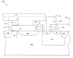
Raised photodiode sensor to increase fill factor and quantum efficiency in scaled pixels
PatentActiveUS20060175641A1
Innovation
- The use of a doped, hydrogenated amorphous silicon photosensor raised above the substrate surface, combined with inert implants like fluorine or deuterium, increases the fill factor and quantum efficiency by reducing leakage and barrier issues, and mitigates hysteresis effects.
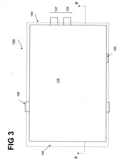
Implementation of avalanche photo diodes in (BI) CMOS processes
PatentInactiveUS20090065704A1
Innovation
- The use of shallow trench isolation technology to form a trench around the p-doped region of the photodiode, filled with a dielectric or metal material, reduces pn junction curvature and electric field strength at the edges, preventing premature breakdown and enhancing the sensitive area and detection efficiency.
Microscopy Image Processing Advancements
Recent advancements in microscopy image processing have significantly enhanced the capabilities of photodiodes in microscopy techniques. These developments have focused on optimizing signal processing algorithms, improving noise reduction techniques, and enhancing image reconstruction methods.
One of the key areas of progress has been in the development of advanced signal processing algorithms specifically tailored for photodiode outputs in microscopy applications. These algorithms have been designed to extract maximum information from the detected light signals, even in low-light conditions. By employing sophisticated mathematical models and machine learning techniques, researchers have been able to improve the signal-to-noise ratio and increase the overall sensitivity of photodiode-based imaging systems.
Noise reduction techniques have also seen substantial improvements. New methods for identifying and filtering out various types of noise, such as shot noise and thermal noise, have been implemented. These techniques often combine hardware-based solutions with software algorithms to achieve optimal results. For instance, the use of cooled photodiodes in conjunction with advanced digital filtering has led to significant reductions in noise levels, allowing for clearer and more detailed microscopy images.
Image reconstruction methods have evolved to take full advantage of the improved photodiode functionalities. Novel algorithms now allow for the reconstruction of high-resolution images from multiple low-resolution captures, effectively increasing the spatial resolution beyond the physical limitations of the photodiode array. This has been particularly beneficial in applications such as super-resolution microscopy, where the ability to resolve fine details is crucial.
The integration of artificial intelligence and machine learning into microscopy image processing has opened up new possibilities for photodiode optimization. AI-powered systems can now adaptively adjust photodiode settings in real-time based on the specific characteristics of the sample being imaged. This dynamic optimization ensures that the best possible image quality is achieved under varying conditions.
Furthermore, advancements in computational imaging techniques have enabled the extraction of more information from photodiode signals than ever before. By combining multiple exposures or utilizing specialized illumination patterns, researchers can now recover depth information, spectral data, and other properties that were previously difficult or impossible to obtain with traditional microscopy methods.
These developments in microscopy image processing have not only improved the quality and information content of microscopy images but have also expanded the range of applications for photodiode-based microscopy systems. From live cell imaging to materials science, the enhanced capabilities of photodiodes are driving new discoveries and pushing the boundaries of what is possible in microscopic analysis.
Regulatory Standards for Scientific Instruments
Regulatory standards play a crucial role in ensuring the safety, reliability, and performance of scientific instruments used in microscopy techniques. For photodiodes optimized for microscopy applications, several key regulatory bodies and standards are particularly relevant.
The International Electrotechnical Commission (IEC) has established standards specifically addressing the safety and performance of optical radiation measurement devices, including photodiodes. IEC 60825-1 provides guidelines for the safety of laser products, which is pertinent when integrating photodiodes into laser-based microscopy systems. Additionally, IEC 61010-1 sets safety requirements for electrical equipment used in measurement, control, and laboratory applications.
In the United States, the Food and Drug Administration (FDA) regulates medical devices, including those used in microscopy. The FDA's Center for Devices and Radiological Health (CDRH) oversees the safety and effectiveness of medical devices, which may include advanced microscopy systems incorporating optimized photodiodes. Manufacturers must comply with the FDA's Quality System Regulation (21 CFR Part 820) and may need to obtain premarket approval or clearance for certain devices.
The European Union's regulatory framework includes the Medical Device Regulation (MDR) and In Vitro Diagnostic Regulation (IVDR), which apply to microscopy instruments used in medical diagnostics. These regulations mandate conformity assessment procedures, clinical evaluations, and post-market surveillance for medical devices, including those utilizing advanced photodiode technologies.
ISO standards also play a significant role in the development and manufacturing of scientific instruments. ISO 13485 specifies requirements for quality management systems in the medical device industry, while ISO 14971 provides guidelines for risk management in medical devices. These standards are essential for ensuring the quality and safety of microscopy instruments incorporating optimized photodiodes.
Electromagnetic compatibility (EMC) regulations, such as those outlined in IEC 61326-1, are crucial for scientific instruments to prevent electromagnetic interference. Photodiodes and associated electronics must comply with these standards to ensure reliable operation in various laboratory environments.
As microscopy techniques advance and incorporate more sophisticated photodiode functionalities, regulatory bodies continue to evolve their standards. For instance, the increasing use of artificial intelligence and machine learning in image analysis has prompted discussions on regulatory approaches for AI-enabled medical devices, which may impact future standards for advanced microscopy systems.
Manufacturers and researchers working on optimizing photodiode functionalities for microscopy techniques must stay informed about these regulatory standards and any updates to ensure compliance throughout the development and commercialization process. Adherence to these standards not only ensures legal compliance but also contributes to the overall quality, safety, and reliability of microscopy instruments in scientific and medical applications.
Unlock deeper insights with Patsnap Eureka Quick Research — get a full tech report to explore trends and direct your research. Try now!
Generate Your Research Report Instantly with AI Agent
Supercharge your innovation with Patsnap Eureka AI Agent Platform!