Photodiode applications in nanotechnology-based sensing platforms
AUG 21, 20259 MIN READ
Generate Your Research Report Instantly with AI Agent
Patsnap Eureka helps you evaluate technical feasibility & market potential.
Photodiode Nanosensing Evolution and Objectives
Photodiodes have played a pivotal role in the evolution of nanotechnology-based sensing platforms, revolutionizing the field of optical detection at the nanoscale. The journey of photodiode integration into nanosensing began in the early 2000s, driven by the increasing demand for miniaturized, highly sensitive, and rapid detection systems. As nanotechnology advanced, researchers recognized the potential of combining photodiodes with nanomaterials to enhance sensing capabilities.
The initial phase of photodiode nanosensing focused on improving sensitivity and response time. Researchers explored various nanomaterials, such as quantum dots and carbon nanotubes, to enhance light absorption and charge carrier generation. This led to the development of hybrid photodiode-nanostructure sensors capable of detecting trace amounts of analytes with unprecedented speed and accuracy.
As the field progressed, the emphasis shifted towards expanding the range of detectable substances and improving selectivity. Scientists began incorporating functionalized nanoparticles and biomolecules onto photodiode surfaces, enabling the detection of specific chemical and biological agents. This breakthrough opened up new possibilities in environmental monitoring, medical diagnostics, and security applications.
The mid-2010s saw a surge in research aimed at overcoming limitations in traditional photodiode designs. Novel architectures, such as nanowire arrays and plasmonic nanostructures, were integrated with photodiodes to enhance light trapping and amplify weak signals. These advancements pushed the boundaries of detection limits, allowing for single-molecule sensing in some cases.
Recent years have witnessed a focus on developing multifunctional nanosensing platforms. Researchers are now combining photodiodes with other sensing modalities, such as electrochemical and mechanical sensors, to create versatile devices capable of simultaneous multi-analyte detection. This trend aligns with the growing need for comprehensive, real-time monitoring in various fields, including healthcare and environmental science.
Looking ahead, the objectives for photodiode applications in nanotechnology-based sensing platforms are ambitious and multifaceted. Key goals include further miniaturization to enable integration into wearable and implantable devices, enhancing specificity to reduce false positives in complex sample matrices, and improving energy efficiency to support long-term, autonomous operation. Additionally, there is a strong push towards developing scalable manufacturing processes to transition these advanced sensors from laboratory prototypes to commercially viable products.
Another critical objective is the development of AI-enhanced data processing algorithms to interpret the complex signals generated by these sophisticated nanosensors. This integration of artificial intelligence with photodiode nanosensing platforms aims to enable real-time, automated decision-making in applications ranging from personalized medicine to smart environmental monitoring systems.
Market Demand Analysis for Nano-Photodiode Sensors
The market demand for nano-photodiode sensors is experiencing significant growth, driven by the increasing need for high-precision, miniaturized sensing solutions across various industries. The global nanosensor market, which includes nano-photodiode sensors, is projected to reach substantial market value in the coming years, with a compound annual growth rate (CAGR) outpacing many other technology sectors.
Key industries fueling this demand include healthcare, environmental monitoring, consumer electronics, and industrial automation. In healthcare, nano-photodiode sensors are finding applications in point-of-care diagnostics, wearable health monitors, and advanced imaging systems. The ability of these sensors to detect minute changes in light intensity and wavelength makes them invaluable for early disease detection and continuous health monitoring.
Environmental monitoring represents another significant market segment. Nano-photodiode sensors are being integrated into air and water quality monitoring systems, offering real-time, highly sensitive detection of pollutants and contaminants. This aligns with growing global concerns about environmental protection and stringent regulations on emissions and water quality.
In the consumer electronics sector, demand is driven by the trend towards more sophisticated and feature-rich devices. Nano-photodiode sensors are being incorporated into smartphones for improved camera performance, ambient light sensing, and even biometric authentication systems. The automotive industry is also adopting these sensors for advanced driver assistance systems (ADAS) and autonomous vehicle technologies.
Industrial automation and the Internet of Things (IoT) are creating new opportunities for nano-photodiode sensors. These sensors are crucial in developing smart factories, where they can be used for quality control, process monitoring, and predictive maintenance. The ability to integrate these sensors into compact, low-power devices makes them ideal for widespread deployment in IoT networks.
Despite the positive market outlook, challenges remain. The high cost of production and the need for specialized manufacturing processes can limit widespread adoption. Additionally, concerns about long-term stability and reliability in harsh environments need to be addressed to expand market penetration in certain industries.
Looking ahead, the market for nano-photodiode sensors is expected to continue its growth trajectory. Advancements in nanotechnology and materials science are likely to enhance sensor performance and reduce production costs, further driving adoption across industries. As the technology matures and becomes more accessible, new applications and market opportunities are expected to emerge, solidifying the position of nano-photodiode sensors as a critical component in the evolving landscape of sensing technologies.
Nanotechnology Challenges in Photodiode Integration
The integration of photodiodes into nanotechnology-based sensing platforms presents several significant challenges that researchers and engineers must overcome. One of the primary obstacles is the miniaturization of photodiodes while maintaining their performance characteristics. As sensing platforms shrink to nanoscale dimensions, traditional photodiode designs struggle to maintain efficiency and sensitivity.
Quantum effects become increasingly prominent at the nanoscale, leading to unpredictable behavior in photodiode performance. These effects can alter the band structure of semiconductor materials, affecting charge carrier generation and transport. Consequently, the quantum confinement effect can significantly impact the spectral response and detection efficiency of nanostructured photodiodes.
Another critical challenge is the integration of nanoscale photodiodes with other components of the sensing platform. The interface between the photodiode and surrounding nanostructures must be carefully engineered to ensure efficient charge transfer and minimal signal loss. This integration often requires novel fabrication techniques and materials that can withstand the harsh conditions of nanoscale manufacturing processes.
Surface effects play a crucial role in nanoscale photodiodes, as the surface-to-volume ratio increases dramatically. Surface states and defects can act as recombination centers, reducing the overall quantum efficiency of the device. Passivation techniques must be developed to mitigate these surface effects without compromising the photodiode's functionality or increasing its size beyond the nanoscale regime.
The choice of materials for nanoscale photodiodes presents another challenge. Traditional semiconductor materials may not exhibit the same properties at the nanoscale, necessitating the exploration of novel materials such as quantum dots, carbon nanotubes, or two-dimensional materials like graphene. These materials offer unique optical and electrical properties but require extensive research to optimize their integration into functional photodiode structures.
Noise reduction becomes increasingly difficult as the dimensions of photodiodes shrink. Thermal noise, shot noise, and other sources of electrical fluctuations can overwhelm the weak signals generated by nanoscale sensing events. Advanced noise suppression techniques and signal processing algorithms must be developed to extract meaningful data from these miniaturized photodiodes.
Lastly, the reliability and long-term stability of nanoscale photodiodes in sensing platforms remain significant concerns. Nanostructures are inherently more susceptible to environmental factors such as temperature fluctuations, mechanical stress, and chemical interactions. Ensuring consistent performance over extended periods and under varying conditions is crucial for the practical implementation of these devices in real-world sensing applications.
Current Nano-Photodiode Sensing Solutions
01 Photodiode structure and fabrication
This category focuses on the physical structure and manufacturing processes of photodiodes. It includes innovations in semiconductor materials, layer compositions, and fabrication techniques to enhance performance and efficiency. Advancements in this area aim to improve light sensitivity, reduce dark current, and optimize overall photodiode characteristics.- Photodiode structure and fabrication: This category focuses on the physical structure and manufacturing processes of photodiodes. It includes innovations in semiconductor materials, layer compositions, and fabrication techniques to enhance photodiode performance, sensitivity, and efficiency. These advancements aim to improve light detection capabilities and reduce noise in various applications.
- Photodiode arrays and imaging systems: This area covers the development of photodiode arrays and their integration into imaging systems. It includes advancements in pixel design, readout circuits, and signal processing for applications such as digital cameras, medical imaging devices, and scientific instruments. The focus is on improving image quality, resolution, and sensitivity in various lighting conditions.
- Avalanche photodiodes: Avalanche photodiodes (APDs) are a specific type of photodiode designed for high-sensitivity light detection. This category encompasses innovations in APD design, including improvements in gain mechanisms, noise reduction, and operating voltage optimization. These developments aim to enhance the performance of APDs in applications such as optical communication and low-light imaging.
- Photodiode applications in optical communication: This category focuses on the use of photodiodes in optical communication systems. It includes advancements in high-speed photodetectors, integrated optical receivers, and related circuitry for fiber-optic networks. The emphasis is on improving data transmission rates, signal quality, and overall system performance in optical communication infrastructure.
- Photodiode-based sensors and instrumentation: This area covers the application of photodiodes in various sensing and instrumentation devices. It includes innovations in light sensors, spectrophotometers, and other analytical instruments that utilize photodiodes for measurement and detection purposes. The focus is on improving sensitivity, accuracy, and versatility of photodiode-based sensors across different industries and scientific fields.
02 Photodiode applications in imaging and sensing
Photodiodes are widely used in various imaging and sensing applications. This category covers innovations related to integrating photodiodes into image sensors, light detection systems, and other optical sensing devices. It includes advancements in pixel design, readout circuits, and signal processing techniques to improve image quality and sensing capabilities.Expand Specific Solutions03 Avalanche photodiodes and high-speed applications
This category focuses on avalanche photodiodes (APDs) and their use in high-speed applications. It includes developments in APD design, gain mechanisms, and noise reduction techniques. These advancements aim to improve the sensitivity and response time of photodiodes for applications such as optical communications and LiDAR systems.Expand Specific Solutions04 Integration of photodiodes with other components
This category covers innovations related to integrating photodiodes with other electronic or optical components. It includes advancements in hybrid and monolithic integration techniques, such as combining photodiodes with amplifiers, filters, or waveguides. These developments aim to create more compact and efficient optoelectronic systems.Expand Specific Solutions05 Specialized photodiode designs
This category encompasses unique and specialized photodiode designs for specific applications or performance requirements. It includes innovations such as back-illuminated photodiodes, organic photodiodes, and photodiodes optimized for particular wavelength ranges. These designs aim to address specific challenges or improve performance in niche applications.Expand Specific Solutions
Key Players in Nano-Photodiode Sensor Industry
The photodiode applications in nanotechnology-based sensing platforms market is in a growth phase, driven by increasing demand for miniaturized and highly sensitive sensors across various industries. The global market size is projected to expand significantly in the coming years, fueled by advancements in nanotechnology and rising adoption in healthcare, environmental monitoring, and industrial applications. While the technology is maturing, there is still room for innovation. Key players like Samsung Electronics, NXP Semiconductors, and BOE Technology are investing heavily in R&D to enhance photodiode performance and integration capabilities. Emerging companies such as OneD Material and Artilux are also making strides in developing novel nanostructured photodiodes, indicating a competitive and dynamic landscape.
OSRAM Opto Semiconductors GmbH
Technical Solution: OSRAM Opto Semiconductors has developed innovative photodiode technologies for nanotechnology-based sensing platforms. Their SFH 2440 L photodiode, designed for biosensors and spectrometers, features a large active area and high sensitivity in the visible to near-infrared range[1]. OSRAM's SFH 2701 silicon PIN photodiode offers fast response times and low capacitance, making it suitable for high-speed optical sensing in nanotech applications[2]. The company has also introduced the SFH 2200 FA, a highly sensitive photodiode with integrated optical filter, ideal for fluorescence detection in nano-biosensing platforms[3]. OSRAM's photodiodes incorporate advanced packaging technologies to minimize crosstalk and maximize light collection efficiency in densely integrated nanosensors[4].
Strengths: High sensitivity, fast response times, and specialized designs for specific nanotech applications. Weaknesses: Limited options for far-infrared detection, which may be required in some nanotechnology sensing scenarios.
Stmicroelectronics Srl
Technical Solution: STMicroelectronics has developed cutting-edge photodiode technologies for nanotechnology-based sensing platforms. Their VD5V0235H photodiode features a small form factor and high responsivity, making it ideal for integration into compact nanosensors[1]. ST's VD6283TX multi-spectral sensor combines multiple photodiodes with on-chip optical filters, enabling simultaneous detection of different wavelengths in a single package, crucial for advanced nanotech sensing applications[2]. The company has also introduced the VL53L5CX, a time-of-flight sensor incorporating an array of single-photon avalanche diodes (SPADs), providing high-resolution 3D sensing capabilities for nanoscale object detection and mapping[3]. ST's silicon photomultipliers (SiPMs) offer extremely high sensitivity and fast timing resolution, suitable for detecting weak optical signals in nanotechnology research[4].
Strengths: Diverse product range, high integration capabilities, and advanced packaging technologies. Weaknesses: Some specialized nanotech applications may require custom solutions beyond the standard product offerings.
Core Innovations in Nano-Photodiode Technology
Photodiode for near infrared detection and method for manufacturing the same
PatentActiveKR1020240082764A
Innovation
- A photodiode design that forms an interface defect at the junction between a semiconductor substrate and a thin film without damaging the substrate, allowing electrons generated in the depletion region to move to the electrode, using a conductive n-type semiconductor thin film and a scattering pattern to diffuse and reflect light, and blocking oxygen injection to create interfacial defects.
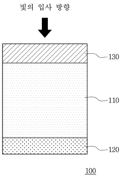
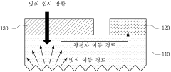
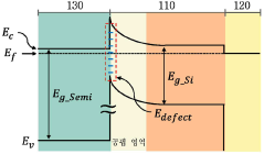
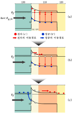
Image sensor and electronic device including the same
PatentActiveUS20170125485A1
Innovation
- An image sensor design incorporating a semiconductor substrate with a nanopattern layer featuring dielectric substances of different refractive indices, allowing for wavelength selectivity and eliminating the need for organic color filters, thereby enhancing sensitivity and reducing pixel size.
Nanomaterial Impact on Photodiode Performance
The integration of nanomaterials into photodiode structures has revolutionized the field of sensing technology, offering unprecedented improvements in device performance and capabilities. Nanomaterials, with their unique physical and chemical properties, have significantly enhanced the sensitivity, selectivity, and response time of photodiodes, making them ideal for a wide range of applications in nanotechnology-based sensing platforms.
One of the most notable impacts of nanomaterials on photodiode performance is the dramatic increase in surface area-to-volume ratio. This characteristic allows for more efficient light absorption and charge carrier generation, resulting in higher photocurrent and improved overall sensitivity. For instance, the incorporation of quantum dots or nanoparticles into the active layer of photodiodes has been shown to extend the spectral response range and increase the quantum efficiency of these devices.
Nanomaterials also contribute to enhanced charge carrier mobility and reduced recombination rates within photodiodes. Carbon nanotubes and graphene, for example, exhibit exceptional electron mobility, facilitating faster charge transport and reducing response times. This improvement is particularly crucial for high-speed sensing applications, such as in optical communication systems or real-time environmental monitoring.
The tunability of nanomaterials' optical and electronic properties offers another significant advantage in photodiode design. By adjusting the size, shape, and composition of nanostructures, researchers can tailor the absorption spectrum and band gap of photodiodes to match specific sensing requirements. This flexibility enables the development of highly selective sensors capable of detecting specific wavelengths or chemical species with great precision.
Furthermore, nanomaterials have enabled the creation of novel photodiode architectures that were previously unattainable. For example, the development of three-dimensional nanostructured photodiodes, such as those based on nanowire arrays or nanoparticle assemblies, has led to devices with superior light-trapping capabilities and enhanced photocurrent generation. These innovative designs push the boundaries of conventional planar photodiode structures, opening up new possibilities for ultra-sensitive and miniaturized sensing platforms.
The integration of plasmonic nanostructures with photodiodes has also emerged as a promising approach to boost device performance. Surface plasmon resonance effects can significantly enhance local electromagnetic fields, leading to improved light absorption and increased photocurrent generation. This phenomenon has been successfully exploited in the development of highly sensitive biosensors and chemical detectors based on plasmonic-enhanced photodiodes.
Scalability of Nano-Photodiode Sensing Platforms
The scalability of nano-photodiode sensing platforms is a critical factor in their widespread adoption and commercial viability. As these platforms continue to evolve, their ability to be scaled up for mass production while maintaining performance and cost-effectiveness becomes increasingly important.
One of the key advantages of nano-photodiode sensing platforms is their potential for miniaturization. This allows for the development of compact, portable devices that can be easily integrated into various applications. However, scaling up production while maintaining the precise nanoscale structures required for optimal performance presents significant challenges.
Advancements in nanofabrication techniques have played a crucial role in improving the scalability of these platforms. Techniques such as electron beam lithography and nanoimprint lithography have enabled the production of uniform and reproducible nanostructures on a larger scale. These methods allow for the creation of highly sensitive and selective nano-photodiode arrays with consistent performance across multiple devices.
The integration of nano-photodiodes with complementary metal-oxide-semiconductor (CMOS) technology has also contributed to improved scalability. CMOS compatibility allows for the incorporation of nano-photodiodes into existing semiconductor manufacturing processes, facilitating large-scale production and reducing costs.
Another factor contributing to the scalability of nano-photodiode sensing platforms is the development of novel materials and architectures. For example, the use of quantum dots and plasmonic nanostructures has led to enhanced sensitivity and selectivity, while also offering potential for easier large-scale fabrication compared to traditional semiconductor-based photodiodes.
Despite these advancements, challenges remain in scaling up nano-photodiode sensing platforms. Issues such as maintaining uniformity across large arrays, optimizing signal-to-noise ratios, and ensuring long-term stability and reliability need to be addressed. Additionally, the development of standardized fabrication processes and quality control measures is essential for consistent performance across mass-produced devices.
As research in this field progresses, new approaches to improve scalability are emerging. These include the exploration of self-assembly techniques for nanostructure formation, the development of flexible and printable nano-photodiode arrays, and the integration of artificial intelligence for automated quality control and performance optimization.
Unlock deeper insights with Patsnap Eureka Quick Research — get a full tech report to explore trends and direct your research. Try now!
Generate Your Research Report Instantly with AI Agent
Supercharge your innovation with Patsnap Eureka AI Agent Platform!