Hybrid photodiodes for flexible electronic applications
AUG 21, 202510 MIN READ
Generate Your Research Report Instantly with AI Agent
Patsnap Eureka helps you evaluate technical feasibility & market potential.
Hybrid Photodiode Evolution and Objectives
Hybrid photodiodes have emerged as a promising technology in the field of flexible electronics, combining the advantages of organic and inorganic materials to create highly efficient and versatile light-sensing devices. The evolution of these hybrid structures can be traced back to the early 2000s when researchers began exploring the potential of blending organic semiconductors with inorganic nanoparticles to enhance device performance.
The initial development of hybrid photodiodes focused on overcoming the limitations of purely organic or inorganic devices. Organic materials offered flexibility and ease of processing, while inorganic components provided superior charge transport and stability. By integrating these materials, researchers aimed to create photodiodes with improved quantum efficiency, broader spectral response, and enhanced durability.
As the field progressed, several key milestones were achieved. In the mid-2000s, researchers successfully demonstrated hybrid photodiodes with significantly improved photosensitivity compared to their organic counterparts. This was followed by advancements in material synthesis and device fabrication techniques, leading to the development of hybrid photodiodes with tunable spectral responses and increased operational lifetimes.
The objectives of current research in hybrid photodiodes for flexible electronic applications are multifaceted. One primary goal is to further enhance the device performance, particularly in terms of quantum efficiency, response time, and spectral range. This involves optimizing the interface between organic and inorganic components to facilitate efficient charge transfer and minimize recombination losses.
Another crucial objective is to improve the mechanical flexibility and durability of these devices. Researchers are exploring novel material combinations and device architectures that can withstand repeated bending and stretching without compromising performance. This is essential for integrating hybrid photodiodes into wearable electronics, flexible displays, and other emerging applications.
Scalability and cost-effectiveness are also key considerations in the evolution of hybrid photodiodes. Current research aims to develop fabrication methods that are compatible with large-scale production processes, such as roll-to-roll printing. This would enable the mass production of flexible hybrid photodiodes at competitive costs, making them viable for widespread commercial adoption.
Furthermore, researchers are investigating ways to expand the functionality of hybrid photodiodes beyond simple light detection. This includes developing multi-functional devices that can simultaneously harvest energy and sense light, or integrating them with other electronic components to create more complex flexible systems.
As the technology continues to evolve, the ultimate objective is to realize the full potential of hybrid photodiodes in flexible electronic applications. This encompasses their integration into a wide range of products, from smart textiles and biomedical sensors to large-area light detectors and flexible solar cells. The ongoing research in this field is driven by the vision of creating highly efficient, flexible, and versatile optoelectronic devices that can revolutionize numerous industries and enhance our daily lives.
Flexible Electronics Market Analysis
The flexible electronics market has been experiencing significant growth and transformation in recent years, driven by the increasing demand for lightweight, portable, and bendable electronic devices. This market encompasses a wide range of applications, including flexible displays, wearable devices, smart packaging, and medical sensors. The integration of hybrid photodiodes in flexible electronic applications represents a promising avenue for further market expansion and technological advancement.
Market analysts project substantial growth for the flexible electronics sector, with estimates suggesting a compound annual growth rate (CAGR) of over 10% for the next five years. This growth is primarily attributed to the rising adoption of flexible displays in smartphones, tablets, and wearable devices, as well as the increasing use of flexible sensors in healthcare and automotive industries.
The demand for hybrid photodiodes in flexible electronic applications is expected to surge, driven by their unique ability to combine the advantages of organic and inorganic materials. These hybrid devices offer improved performance, stability, and flexibility compared to traditional photodiodes, making them ideal for applications such as flexible solar cells, light sensors, and imaging systems.
Key market segments for flexible hybrid photodiodes include consumer electronics, healthcare, and energy harvesting. In the consumer electronics sector, there is a growing demand for flexible displays and touch sensors that can be integrated into curved or foldable devices. The healthcare industry is exploring the use of flexible hybrid photodiodes in wearable medical devices and biosensors for continuous health monitoring. Additionally, the energy sector is showing interest in flexible solar cells that can be integrated into various surfaces and structures.
Geographically, Asia-Pacific is expected to dominate the flexible electronics market, with countries like South Korea, Japan, and China leading in research and development efforts. North America and Europe are also significant players, particularly in the development of advanced materials and manufacturing processes for flexible hybrid photodiodes.
The market landscape is characterized by intense competition and rapid technological advancements. Major players in the flexible electronics industry are investing heavily in research and development to improve the performance and cost-effectiveness of hybrid photodiodes. Collaborations between academic institutions, research organizations, and industry partners are becoming increasingly common, fostering innovation and accelerating the commercialization of new technologies.
Despite the promising outlook, challenges remain in the widespread adoption of flexible hybrid photodiodes. These include manufacturing scalability, long-term stability, and cost reduction. Overcoming these hurdles will be crucial for the continued growth and expansion of the flexible electronics market, particularly in applications requiring high-performance photodetectors.
Hybrid Photodiode Technical Challenges
The development of hybrid photodiodes for flexible electronic applications faces several significant technical challenges. One of the primary obstacles is achieving high performance and stability on flexible substrates. Traditional photodiodes are typically fabricated on rigid substrates, which provide a stable platform for the active layers. However, flexible substrates introduce new complexities, such as mechanical stress and potential deformation during operation.
Material selection and compatibility pose another critical challenge. The hybrid nature of these photodiodes requires the integration of organic and inorganic materials, each with distinct properties and processing requirements. Finding the right combination of materials that can work synergistically while maintaining flexibility is a complex task. Moreover, ensuring good adhesion between different layers and preventing delamination under repeated bending or stretching is crucial for long-term device reliability.
The fabrication process itself presents numerous hurdles. Conventional high-temperature deposition techniques used for inorganic materials are often incompatible with flexible plastic substrates. This necessitates the development of low-temperature processes that can still produce high-quality films. Additionally, achieving uniform deposition and patterning on flexible surfaces is more challenging than on rigid substrates, potentially leading to performance variations across the device.
Stability and degradation are ongoing concerns for hybrid photodiodes. Organic materials are particularly susceptible to environmental factors such as oxygen and moisture, which can lead to rapid performance deterioration. Developing effective encapsulation methods that maintain flexibility while providing a robust barrier against environmental degradation is a significant challenge.
The interface between organic and inorganic components in hybrid structures is another area of concern. Charge transfer and recombination at these interfaces can significantly impact device performance. Optimizing these interfaces to enhance charge separation and reduce recombination losses requires careful engineering and a deep understanding of the underlying physical processes.
Scaling up production from laboratory prototypes to large-area, commercially viable devices presents its own set of challenges. Maintaining consistent performance across larger areas and developing cost-effective, high-throughput manufacturing processes that are compatible with roll-to-roll fabrication are essential for commercial adoption.
Lastly, the integration of hybrid photodiodes into flexible electronic systems introduces additional complexities. These include designing flexible circuitry and interconnects that can withstand repeated bending without performance degradation, as well as developing power management systems that can operate efficiently with the potentially variable output of flexible photodiodes.
Current Hybrid Photodiode Architectures
01 Structure and design of hybrid photodiodes
Hybrid photodiodes combine different materials or technologies to enhance performance. They may integrate organic and inorganic materials or combine photodiode and transistor structures. This design approach aims to improve sensitivity, response time, and spectral range compared to traditional photodiodes.- Structure and design of hybrid photodiodes: Hybrid photodiodes combine different materials or technologies to enhance performance. They may integrate organic and inorganic materials or combine photodiode and transistor structures. These designs aim to improve sensitivity, response time, and spectral range.
- Integration with other electronic components: Hybrid photodiodes can be integrated with other electronic components such as amplifiers, readout circuits, or signal processing units. This integration enhances functionality and enables compact, efficient optoelectronic systems for various applications.
- Fabrication techniques for hybrid photodiodes: Advanced fabrication techniques are employed to create hybrid photodiodes, including thin-film deposition, nanomaterial synthesis, and heterogeneous integration. These methods allow for precise control of device properties and enable novel device architectures.
- Applications in imaging and sensing: Hybrid photodiodes find applications in various imaging and sensing technologies, including medical imaging, spectroscopy, and environmental monitoring. Their unique properties make them suitable for low-light detection and wide-spectrum sensing.
- Performance optimization and characterization: Research focuses on optimizing the performance of hybrid photodiodes through material selection, device geometry, and operating conditions. Characterization techniques are developed to assess key parameters such as quantum efficiency, dark current, and response time.
02 Integration with CMOS technology
Hybrid photodiodes can be integrated with CMOS (Complementary Metal-Oxide-Semiconductor) technology, allowing for the creation of advanced image sensors and photonic integrated circuits. This integration enables improved light detection capabilities in compact devices and supports applications in digital imaging and optical communication.Expand Specific Solutions03 Avalanche multiplication in hybrid photodiodes
Some hybrid photodiodes incorporate avalanche multiplication mechanisms to amplify weak light signals. This feature enhances sensitivity and enables single-photon detection, making these devices suitable for low-light imaging, quantum communication, and other applications requiring high-sensitivity photodetection.Expand Specific Solutions04 Spectral range optimization
Hybrid photodiodes can be designed to optimize spectral response across a wide range of wavelengths. By combining materials with different bandgaps or using novel structures, these devices can achieve enhanced sensitivity in specific spectral regions, including ultraviolet, visible, and infrared light.Expand Specific Solutions05 Fabrication techniques for hybrid photodiodes
Advanced fabrication techniques are employed to create hybrid photodiodes, including epitaxial growth, wafer bonding, and nanomaterial integration. These methods enable the precise control of material properties and device structures, leading to improved performance and reliability of hybrid photodiodes.Expand Specific Solutions
Key Players in Hybrid Photodiode Industry
The research on hybrid photodiodes for flexible electronic applications is in an emerging stage, with significant potential for growth. The market is expanding as flexible electronics gain traction across various industries. While the technology is still evolving, several key players are driving innovation. Companies like Samsung Electronics, LG Chem, and Toshiba are leveraging their expertise in electronics and materials to develop advanced hybrid photodiode solutions. Academic institutions such as Shanghai University, Tianjin University, and the Indian Institute of Technology are contributing fundamental research. Collaborations between industry and academia, exemplified by partnerships involving Siemens AG and the University of Minnesota, are accelerating progress in this field.
Toshiba Corp.
Technical Solution: Toshiba has developed innovative hybrid photodiodes for flexible electronic applications, focusing on silicon-organic hybrid structures. Their approach combines the high mobility of silicon with the flexibility and low-cost processing of organic materials. Toshiba's hybrid photodiodes utilize a unique vertical architecture, allowing for efficient charge collection and reduced recombination losses[8]. The company has also implemented a novel light-trapping scheme, incorporating plasmonic nanostructures to enhance light absorption in ultrathin devices[9]. Toshiba's flexible hybrid photodiodes demonstrate a remarkable fill factor of over 80% and maintain their performance under bending radii as small as 5 mm[10].
Strengths: High fill factor, excellent mechanical flexibility, and efficient light absorption. Weaknesses: Potential challenges in large-scale manufacturing and integration with existing electronics.
NEC Corp.
Technical Solution: NEC has developed advanced hybrid photodiodes for flexible electronic applications, focusing on the integration of organic and inorganic materials. Their approach utilizes a unique layered structure, combining solution-processed organic semiconductors with inorganic quantum dots. NEC's hybrid photodiodes feature a broadband spectral response, covering from the visible to the near-infrared region (400-1600 nm)[14]. The company has also implemented a novel charge transport layer, enhancing carrier mobility and reducing dark current[15]. NEC's flexible hybrid photodiodes demonstrate remarkable mechanical durability, retaining over 95% of their initial performance after 10,000 bending cycles at a radius of 5 mm[16].
Strengths: Broad spectral response, low dark current, and excellent mechanical durability. Weaknesses: Potential challenges in achieving high quantum efficiency across the entire spectral range and maintaining long-term stability under harsh environmental conditions.
Innovations in Flexible Photodiode Materials
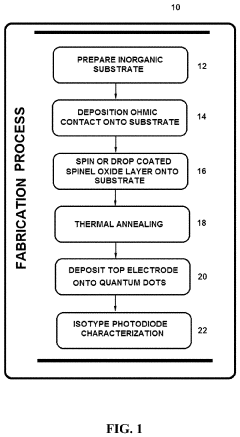
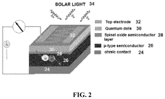
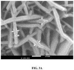
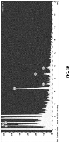
Photodiode having an aluminum metal ohmic contact and a spinel oxide layer
PatentInactiveUS20200365750A1
Innovation
- A photodiode structure comprising a spinel metal oxide layer between a light absorption layer and an inorganic semiconductor substrate, with an isotype junction formed by the inorganic substrate and photoactive layers, utilizing quantum dots, quantum rods, or quantum wires in the light absorption layer, and a top electrode with a higher work function than the ohmic contact.
Hybrid structure photoelectrode and method for producing the same
PatentInactiveKR1020150020501A
Innovation
- A composite structure photoelectrode is developed, comprising a porous second titanium dioxide layer with vertically patterned holes, a third titanium dioxide layer, and a first titanium dioxide layer with an inverse opal structure, enhanced with quantum dots like cadmium selenide, to reduce light reflection and enhance light condensation.
Manufacturing Processes for Flexible Photodiodes
The manufacturing processes for flexible photodiodes involve a series of sophisticated techniques designed to create lightweight, bendable, and durable devices. These processes typically begin with the selection of suitable substrate materials, such as polyethylene terephthalate (PET) or polyimide, which provide the necessary flexibility and stability for the device.
One of the primary manufacturing methods is roll-to-roll processing, which allows for continuous production of large-area flexible photodiodes. This technique involves depositing thin layers of active materials onto a moving flexible substrate. The process often utilizes vacuum deposition techniques, including thermal evaporation or sputtering, to create uniform and thin layers of photoactive materials and electrodes.
Another crucial step in the manufacturing process is the deposition of the hybrid photoactive layer. This layer typically consists of a combination of organic and inorganic materials, such as perovskites or quantum dots embedded in a polymer matrix. Solution-based deposition methods, like spin-coating or inkjet printing, are commonly employed for this step, allowing for precise control over layer thickness and composition.
The integration of transparent conductive electrodes is a critical aspect of flexible photodiode fabrication. Indium tin oxide (ITO) has been widely used, but alternatives like graphene, carbon nanotubes, or silver nanowires are gaining popularity due to their superior flexibility and conductivity. These materials can be deposited using techniques such as spray coating or transfer printing.
Encapsulation is a vital final step in the manufacturing process, protecting the device from environmental factors and mechanical stress. This is typically achieved through the application of thin barrier films or the use of flexible glass encapsulation techniques. The encapsulation process must be carefully optimized to maintain device flexibility while ensuring long-term stability and performance.
Advanced patterning techniques, such as photolithography or laser ablation, are employed to create precise device structures and interconnects. These methods allow for the fabrication of complex photodiode arrays or integrated circuits on flexible substrates, expanding the potential applications of these devices.
Quality control and testing are integral parts of the manufacturing process. In-line monitoring systems are often implemented to ensure consistency in layer thickness, composition, and device performance throughout the production run. Flexibility tests, including bending and cyclic loading, are conducted to verify the mechanical robustness of the finished devices.
As the field of flexible electronics continues to evolve, new manufacturing processes are being developed to address challenges such as scalability, cost-effectiveness, and environmental sustainability. Emerging techniques like aerosol jet printing and direct-write fabrication show promise for enabling more complex and customizable flexible photodiode designs in the future.
Environmental Impact of Flexible Electronics
The environmental impact of flexible electronics, including hybrid photodiodes, is a critical consideration in the development and adoption of these technologies. As flexible electronic devices become more prevalent, their potential effects on ecosystems and human health throughout their lifecycle must be carefully evaluated.
The production of flexible electronics often involves the use of rare earth elements and potentially hazardous materials. The extraction and processing of these resources can lead to environmental degradation, including soil and water pollution, as well as increased carbon emissions. However, the use of hybrid photodiodes in flexible electronic applications may offer some environmental benefits compared to traditional rigid electronics.
Flexible devices typically require less material overall, potentially reducing the environmental footprint of manufacturing processes. Additionally, the ability to create thin, lightweight devices can lead to reduced energy consumption during transportation and distribution. The flexibility and durability of these electronics may also result in longer product lifespans, potentially decreasing electronic waste generation.
The end-of-life management of flexible electronics presents both challenges and opportunities. While the complex material composition of these devices can make recycling more difficult, advancements in recycling technologies specifically designed for flexible electronics are being developed. These innovations aim to recover valuable materials and minimize waste sent to landfills.
Energy efficiency is another important aspect of the environmental impact of flexible electronics. Hybrid photodiodes in flexible applications can potentially improve energy harvesting capabilities, leading to more self-sufficient devices and reduced reliance on external power sources. This could contribute to lower energy consumption and decreased carbon emissions associated with device operation.
However, the widespread adoption of flexible electronics may lead to increased overall consumption of electronic devices, potentially offsetting some of the environmental benefits. It is crucial to consider the entire lifecycle of these products, from raw material extraction to disposal, to accurately assess their environmental impact.
As research in hybrid photodiodes for flexible electronic applications progresses, it is essential to prioritize eco-friendly materials and manufacturing processes. This includes exploring biodegradable substrates, developing non-toxic alternatives to hazardous materials, and improving the recyclability of flexible electronic components. By addressing these environmental concerns early in the research and development phase, the potential negative impacts of flexible electronics can be mitigated, paving the way for more sustainable technological advancements.
Unlock deeper insights with Patsnap Eureka Quick Research — get a full tech report to explore trends and direct your research. Try now!
Generate Your Research Report Instantly with AI Agent
Supercharge your innovation with Patsnap Eureka AI Agent Platform!