Photodiodes coupled with signal amplifiers for telecommunication upgrades
AUG 21, 20259 MIN READ
Generate Your Research Report Instantly with AI Agent
Patsnap Eureka helps you evaluate technical feasibility & market potential.
Photodiode-Amplifier Evolution and Objectives
The evolution of photodiodes coupled with signal amplifiers has been a cornerstone in the advancement of telecommunication systems. This technological pairing has undergone significant transformations since its inception, driven by the ever-increasing demand for faster and more reliable data transmission. The journey began with simple photodiode designs that could detect light signals but struggled with weak electrical outputs, necessitating the development of more sophisticated amplification techniques.
As telecommunications networks expanded and data rates soared, the objectives for photodiode-amplifier systems became increasingly ambitious. The primary goal has been to achieve higher bandwidth and sensitivity while maintaining low noise levels and power consumption. This has led to a series of innovations in both photodiode structures and amplifier designs, each iteration bringing us closer to the ideal of seamless, high-speed optical communication.
The evolution of photodiodes has seen the progression from basic PIN (Positive-Intrinsic-Negative) structures to more advanced designs like avalanche photodiodes (APDs) and, more recently, uni-traveling carrier (UTC) photodiodes. These advancements have significantly improved the speed and sensitivity of light detection, pushing the boundaries of what's possible in optical-to-electrical conversion.
Concurrently, amplifier technology has evolved from simple transistor-based designs to integrated circuits that incorporate multiple stages of amplification and signal processing. The development of transimpedance amplifiers (TIAs) marked a significant milestone, offering a balance between high gain and wide bandwidth. Recent years have seen the emergence of distributed amplifiers and traveling wave amplifiers, which have further extended the frequency range of these systems.
The objectives for future photodiode-amplifier systems are multifaceted. Researchers aim to develop photodiodes with even higher quantum efficiency and lower dark current, while simultaneously reducing their capacitance to allow for faster operation. On the amplifier side, the goals include achieving higher gain-bandwidth products, lower noise figures, and improved linearity, all while reducing power consumption and thermal effects.
Another critical objective is the seamless integration of photodiodes and amplifiers into single-chip solutions. This integration aims to minimize parasitic effects, reduce overall system size, and improve reliability. Additionally, there's a growing focus on developing systems that can operate across a wider range of wavelengths, supporting the move towards wavelength division multiplexing (WDM) in optical networks.
As we look to the future, the overarching goal is to enable telecommunication systems that can handle the exponential growth in data traffic while meeting the stringent requirements of emerging applications such as 5G and beyond, Internet of Things (IoT), and high-definition video streaming. This necessitates continued innovation in photodiode-amplifier technology to achieve unprecedented levels of performance, efficiency, and reliability.
Telecom Market Demand Analysis
The telecommunications market is experiencing a significant surge in demand for advanced photodiode and signal amplifier technologies, driven by the ever-increasing need for faster, more reliable, and higher-capacity communication networks. As global data traffic continues to grow exponentially, telecom operators are under pressure to upgrade their infrastructure to meet the demands of emerging technologies such as 5G, Internet of Things (IoT), and cloud computing.
The market for photodiodes coupled with signal amplifiers in the telecom sector is projected to grow substantially over the next five years. This growth is primarily fueled by the rapid expansion of fiber-optic networks, which require high-performance photodetectors and amplifiers to convert optical signals into electrical signals efficiently. The increasing adoption of fiber-to-the-home (FTTH) and fiber-to-the-premises (FTTP) solutions in both developed and developing countries is a key driver for this market segment.
Telecom operators are particularly interested in photodiodes and signal amplifiers that can support higher data rates and longer transmission distances. There is a growing demand for components that can operate in the 100G, 400G, and even 800G transmission ranges, as network providers seek to increase bandwidth capacity to meet the needs of data-intensive applications and services.
The market is also seeing increased demand for integrated photonic solutions that combine photodiodes, amplifiers, and other optical components on a single chip. These integrated solutions offer benefits such as reduced power consumption, smaller form factors, and improved signal integrity, which are crucial for next-generation telecom infrastructure.
Another significant trend driving market demand is the push for energy-efficient technologies. Telecom operators are looking for photodiodes and amplifiers that can deliver high performance while minimizing power consumption, as energy costs represent a substantial portion of operational expenses for network providers.
In terms of geographical distribution, the Asia-Pacific region is expected to show the highest growth rate in demand for these technologies, driven by rapid infrastructure development and increasing internet penetration in countries like China and India. North America and Europe continue to be significant markets, with a focus on upgrading existing networks to support advanced services and applications.
The demand for ruggedized and environmentally robust photodiodes and amplifiers is also on the rise, particularly for applications in harsh environments such as undersea cables and remote terrestrial locations. This trend is driven by the expansion of global connectivity initiatives and the need for reliable communication links in challenging conditions.
As telecom networks evolve towards software-defined networking (SDN) and network function virtualization (NFV), there is a growing interest in photodiodes and amplifiers that can support flexible and programmable optical networks. This demand is pushing manufacturers to develop more versatile and adaptable components that can be easily integrated into dynamic network architectures.
Current Challenges in Optical Signal Amplification
The field of optical signal amplification in telecommunications faces several significant challenges that hinder the advancement of high-speed, long-distance data transmission. One of the primary issues is the inherent noise introduced during the amplification process. As signals travel through optical fibers, they naturally attenuate, requiring periodic amplification. However, each amplification stage introduces additional noise, primarily in the form of amplified spontaneous emission (ASE), which degrades the signal-to-noise ratio (SNR) and limits the overall system performance.
Another critical challenge is the management of nonlinear effects in optical fibers. As signal power increases, phenomena such as self-phase modulation, cross-phase modulation, and four-wave mixing become more pronounced. These nonlinear effects can cause signal distortion, inter-channel interference, and spectral broadening, all of which compromise the integrity of the transmitted data and limit the capacity of optical communication systems.
The bandwidth limitations of current amplification technologies also present a significant hurdle. While the demand for data transmission continues to grow exponentially, the usable bandwidth of erbium-doped fiber amplifiers (EDFAs), the most widely deployed optical amplifiers, is restricted to the C-band and L-band. This constraint creates a bottleneck in the overall capacity of optical networks, prompting the need for more efficient amplification techniques or the exploration of new spectral regions.
Power consumption and heat dissipation remain ongoing concerns in optical signal amplification. As network operators strive for higher data rates and longer transmission distances, the energy requirements for signal amplification increase substantially. This not only raises operational costs but also presents challenges in terms of system reliability and environmental impact, particularly in submarine cable systems where power delivery is limited.
The integration of advanced modulation formats and coherent detection schemes with existing amplification technologies poses another set of challenges. These sophisticated transmission techniques require precise management of signal phase and polarization, which can be adversely affected by the amplification process. Maintaining signal fidelity across multiple amplification stages while supporting complex modulation formats is crucial for next-generation high-capacity systems.
Lastly, the development of wideband amplifiers capable of simultaneously amplifying multiple transmission bands is an area of intense research. The goal is to expand the usable spectrum beyond the traditional C and L bands, potentially including the S and U bands. However, achieving flat gain profiles and managing differential group delay across such wide bandwidths presents significant technical hurdles that must be overcome to realize the full potential of wideband amplification in telecommunications networks.
State-of-the-Art Photodiode-Amplifier Solutions
01 Photodiode and amplifier integration
Integration of photodiodes with signal amplifiers on a single chip or in close proximity to improve signal quality and reduce noise. This approach enhances sensitivity and performance in various optoelectronic applications.- Photodiode and amplifier integration: This approach involves integrating photodiodes with signal amplifiers on a single chip or in close proximity. The integration enhances signal quality by reducing noise and improving sensitivity. It allows for compact designs suitable for various applications, including optical communication and imaging systems.
- Transimpedance amplifier configurations: Transimpedance amplifiers are commonly used with photodiodes to convert current signals to voltage. These configurations offer high gain, low noise, and wide bandwidth, making them ideal for amplifying weak photodiode signals. Various circuit topologies are employed to optimize performance for specific applications.
- Automatic gain control in photodiode amplifiers: Automatic gain control mechanisms are implemented in photodiode amplifier circuits to maintain optimal signal levels across varying light intensities. This approach ensures a wide dynamic range and prevents signal saturation or distortion, enhancing the overall performance of the photodetection system.
- Noise reduction techniques in photodiode amplifiers: Various noise reduction techniques are employed in photodiode amplifier designs to improve signal-to-noise ratio. These may include chopper stabilization, correlated double sampling, and differential amplification. Such techniques are crucial for detecting weak optical signals and improving the overall sensitivity of the system.
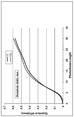
- Multi-stage amplification for photodiodes: Multi-stage amplification architectures are used to achieve high gain and bandwidth in photodiode signal processing. This approach allows for better control over gain distribution and frequency response, enabling the design of high-performance optical receivers for applications such as fiber-optic communications and light detection and ranging (LIDAR) systems.
02 Transimpedance amplifier designs
Specialized transimpedance amplifier configurations optimized for photodiode signal amplification. These designs focus on high gain, low noise, and wide bandwidth to effectively convert the photodiode's current output into a voltage signal.Expand Specific Solutions03 Automatic gain control for photodiode amplifiers
Implementation of automatic gain control mechanisms in photodiode amplifier circuits to maintain optimal signal levels across varying light intensities. This approach improves dynamic range and prevents signal saturation or distortion.Expand Specific Solutions04 Noise reduction techniques in photodiode amplifiers
Various methods to minimize noise in photodiode amplifier systems, including chopper stabilization, correlated double sampling, and advanced filtering techniques. These approaches aim to improve the signal-to-noise ratio and overall sensitivity of the photodetection system.Expand Specific Solutions05 Multi-stage amplification for photodiodes
Utilization of multi-stage amplification architectures to achieve high gain and maintain bandwidth in photodiode signal processing. This approach often involves cascaded amplifier stages with careful consideration of noise contribution and frequency response at each stage.Expand Specific Solutions
Key Players in Optical Communication Industry
The research on photodiodes coupled with signal amplifiers for telecommunication upgrades is in a mature stage of development, with significant market potential due to the growing demand for high-speed data transmission. The global market for these components is substantial, driven by the continuous expansion of telecommunications infrastructure. Key players in this field include Renesas Electronics, Mitsubishi Electric, and Hitachi, who are leveraging their expertise in semiconductor technology to develop advanced photodiode and amplifier solutions. The technology's maturity is evident in the diverse range of applications and the ongoing refinement of existing products by established companies, indicating a competitive landscape with opportunities for innovation in performance and efficiency.
Hamamatsu Photonics KK
Technical Solution: Hamamatsu Photonics has developed advanced photodiodes coupled with high-performance signal amplifiers for telecommunication upgrades. Their technology includes InGaAs PIN photodiodes with ultra-low dark current and high-speed response, integrated with low-noise transimpedance amplifiers (TIAs) [1]. The company's APD (Avalanche Photodiode) modules feature internal high-speed amplifiers, achieving excellent sensitivity and wide dynamic range [2]. Hamamatsu's silicon photomultipliers (SiPMs) combined with custom readout electronics offer high photon detection efficiency and fast timing resolution, suitable for advanced optical communication systems [3]. Their MPPC (Multi-Pixel Photon Counter) technology, when coupled with specialized amplifiers, provides single-photon sensitivity with low crosstalk, making it ideal for long-distance, high-speed optical networks [4].
Strengths: Industry-leading sensitivity and low noise performance, wide range of customizable solutions. Weaknesses: Higher cost compared to some competitors, may require specialized knowledge for optimal integration.
Finisar Corp.
Technical Solution: Finisar Corporation (now part of II-VI Incorporated) has been actively researching photodiodes coupled with signal amplifiers for telecommunication upgrades. Their work includes developing high-speed InGaAs photodetectors integrated with advanced TIAs for 100G and beyond optical transceivers [1]. Finisar has made advancements in APD technology, creating designs with improved sensitivity and reduced noise, paired with specialized amplifier circuits for long-reach optical links [2]. The company has also focused on coherent detection systems, developing integrated photodiode arrays with linear TIAs for advanced modulation formats used in high-capacity networks [3]. Finisar's research extends to silicon photonics, where they've explored hybrid integration of III-V photodiodes with silicon-based amplifiers for next-generation photonic integrated circuits [4].
Strengths: Extensive experience in optical communication components, strong vertical integration capabilities. Weaknesses: Recent merger with II-VI may lead to shifts in research priorities or product focus.
Innovative Photodiode-Amplifier Coupling Techniques
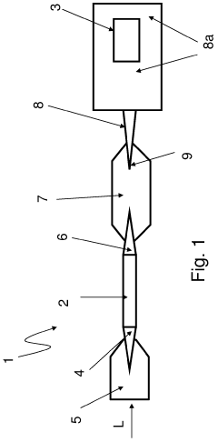
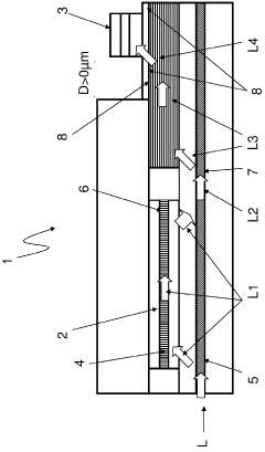
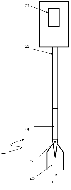
A monolithic integrated structure comprising a buried heterostructure semiconductor optical amplifier and a photodetector
PatentWO2012041850A1
Innovation
- A monolithic integrated structure comprising a buried heterostructure semiconductor optical amplifier with an active waveguide and a deep ridge photodetector, utilizing a high confinement optical passive waveguide for evanescent coupling and spot size converters to enhance coupling efficiency and reduce reflection, while maintaining low polarization dependence and high speed operation.
Optical wireless communication receiver with large photodetector surface area, large field of view and high bandwidth
PatentActiveUS11923900B2
Innovation
- A two-dimensional array of photodiodes is arranged at the focal plane of a lens, with outputs combined and amplified, allowing for a configurable photodetector surface and bandwidth by adjusting the number of parallel branches and cascaded photodiodes, thereby increasing the active area and angular aperture without reducing bandwidth.
Bandwidth and Latency Optimization Strategies
In the realm of telecommunication upgrades, optimizing bandwidth and reducing latency are crucial for enhancing overall system performance. The integration of photodiodes coupled with signal amplifiers presents significant opportunities for achieving these goals. Bandwidth optimization strategies focus on maximizing the amount of data that can be transmitted over a given time period, while latency optimization aims to minimize the delay between data transmission and reception.
One key strategy for bandwidth optimization involves the use of advanced modulation techniques. By employing higher-order modulation schemes, such as Quadrature Amplitude Modulation (QAM) or Orthogonal Frequency-Division Multiplexing (OFDM), the system can transmit more bits per symbol, effectively increasing the data rate without expanding the frequency spectrum. This approach, however, requires careful consideration of signal-to-noise ratio (SNR) to maintain signal integrity.
Implementing wavelength division multiplexing (WDM) is another powerful method for increasing bandwidth. WDM allows multiple optical signals at different wavelengths to be transmitted simultaneously over a single fiber, dramatically increasing the capacity of existing infrastructure. The combination of high-speed photodiodes and low-noise amplifiers is essential for effectively detecting and processing these multiplexed signals.
Latency optimization strategies often focus on reducing processing time and minimizing signal path lengths. One approach involves the use of edge computing architectures, where data processing is performed closer to the source, reducing the distance that signals need to travel. This can be particularly effective when combined with high-speed photodiodes and amplifiers that can quickly convert and boost optical signals.
Advanced signal processing techniques, such as digital signal processing (DSP) and machine learning algorithms, can also contribute to both bandwidth and latency optimization. These methods can help in real-time signal equalization, adaptive modulation, and error correction, improving overall system efficiency and reducing retransmission rates.
The development of ultra-fast photodiodes with high responsivity and low capacitance is crucial for pushing the boundaries of bandwidth and latency optimization. When coupled with high-performance transimpedance amplifiers (TIAs), these photodiodes can achieve exceptional bandwidth-efficiency products, enabling faster and more reliable data transmission.
Lastly, the integration of coherent detection techniques with advanced DSP algorithms offers a promising avenue for further optimization. This approach allows for the extraction of both amplitude and phase information from optical signals, enabling more efficient use of the available spectrum and potentially reducing latency through improved signal recovery and error correction mechanisms.
Energy Efficiency in Optical Communication Systems
Energy efficiency has become a critical concern in optical communication systems as the demand for higher data rates and longer transmission distances continues to grow. The integration of photodiodes coupled with signal amplifiers plays a crucial role in addressing this challenge, offering potential solutions for telecommunication upgrades that prioritize energy conservation.
Photodiodes serve as the primary light-sensing components in optical receivers, converting incoming optical signals into electrical currents. When coupled with signal amplifiers, these devices can significantly enhance the sensitivity and performance of optical communication systems. The key to improving energy efficiency lies in optimizing the design and operation of these integrated components.
One approach to enhancing energy efficiency is the development of high-responsivity photodiodes. These advanced devices can generate stronger electrical signals from weaker optical inputs, reducing the need for subsequent amplification stages. By minimizing the number of amplification stages, the overall power consumption of the system can be reduced without compromising signal quality.
Signal amplifiers, when properly designed and integrated with photodiodes, can further contribute to energy efficiency. Low-noise amplifiers (LNAs) are particularly important in this context, as they can boost weak signals while introducing minimal additional noise. This allows for the detection of weaker optical signals, potentially enabling longer transmission distances or lower-power transmitters.
Recent advancements in semiconductor materials and fabrication techniques have led to the development of novel photodiode structures with improved quantum efficiency and reduced dark current. These innovations contribute to better signal-to-noise ratios and lower power requirements for signal amplification.
The integration of photodiodes and signal amplifiers on a single chip, known as monolithic integration, offers additional benefits in terms of energy efficiency. This approach reduces parasitic capacitances and resistances associated with interconnects, leading to improved high-frequency performance and lower power consumption.
Furthermore, the implementation of adaptive gain control mechanisms in signal amplifiers can optimize power usage based on the strength of incoming signals. This dynamic adjustment ensures that the system operates at the minimum required power level while maintaining reliable communication.
As telecommunications networks continue to expand and evolve, the focus on energy-efficient optical communication systems becomes increasingly important. The ongoing research and development in photodiodes coupled with signal amplifiers promise to deliver significant improvements in both performance and energy conservation, paving the way for more sustainable and cost-effective telecommunication infrastructures.
Unlock deeper insights with Patsnap Eureka Quick Research — get a full tech report to explore trends and direct your research. Try now!
Generate Your Research Report Instantly with AI Agent
Supercharge your innovation with Patsnap Eureka AI Agent Platform!