Photodiode developments in mobile device displays
AUG 21, 20258 MIN READ
Generate Your Research Report Instantly with AI Agent
Patsnap Eureka helps you evaluate technical feasibility & market potential.
Photodiode Evolution
The evolution of photodiodes in mobile device displays represents a significant technological advancement in the field of optoelectronics. This progression has been driven by the increasing demand for more sophisticated and efficient display technologies in smartphones and tablets.
In the early stages of mobile device development, photodiodes were primarily used for ambient light sensing to adjust screen brightness. These simple photodiodes were typically separate components, often placed near the front-facing camera or on the device's bezel.
As display technology advanced, the integration of photodiodes directly into the display panel became a focal point of innovation. This shift was motivated by the desire to maximize screen real estate and improve overall device aesthetics by reducing bezel size. The first attempts at in-display photodiodes faced challenges related to light transmission through the display layers and signal-to-noise ratios.
A major breakthrough came with the development of transparent photodiodes using materials such as indium gallium zinc oxide (IGZO) and amorphous silicon. These materials allowed for the creation of photodiodes that could be integrated into the display stack without significantly impacting display quality or light transmission.
The next phase of evolution saw the miniaturization of photodiodes and their integration into individual pixels. This development enabled more advanced functionalities, such as under-display fingerprint sensing and improved ambient light detection for more precise brightness control.
Recent advancements have focused on enhancing the sensitivity and response time of in-display photodiodes. This has been achieved through the use of novel materials and structures, such as quantum dot-based photodiodes and organic photodiodes (OPDs). These innovations have not only improved the performance of existing applications but also opened up possibilities for new features like in-display cameras and advanced gesture recognition.
The latest trend in photodiode evolution for mobile displays is the development of multi-functional sensors. These advanced photodiodes can simultaneously perform multiple tasks, such as ambient light sensing, proximity detection, and even heart rate monitoring, all integrated seamlessly within the display panel.
Looking forward, the evolution of photodiodes in mobile device displays is expected to continue, with a focus on further improving sensitivity, reducing power consumption, and expanding functionality. This ongoing development will likely lead to more immersive and interactive display experiences in future mobile devices.
Market Demand Analysis
The market demand for photodiodes in mobile device displays has been experiencing significant growth in recent years, driven by the increasing consumer expectations for advanced display technologies and enhanced user experiences. As smartphones and tablets become integral parts of daily life, manufacturers are constantly seeking ways to improve display quality, energy efficiency, and overall device performance.
One of the primary factors fueling the demand for photodiodes in mobile displays is the growing emphasis on ambient light sensing and automatic brightness adjustment. These features not only enhance user comfort but also contribute to battery conservation, addressing a key concern for mobile device users. The ability of photodiodes to accurately detect ambient light levels and adjust screen brightness accordingly has become a standard expectation in mid-range to high-end smartphones and tablets.
Furthermore, the rise of under-display technologies, particularly for front-facing cameras and facial recognition systems, has created a new market segment for specialized photodiodes. These components play a crucial role in enabling seamless integration of sensors beneath the display surface, maintaining the aesthetic appeal of bezel-less designs while preserving functionality.
The automotive industry's increasing adoption of advanced driver-assistance systems (ADAS) and in-vehicle infotainment systems has also contributed to the growing demand for high-performance photodiodes. As mobile display technologies find their way into vehicle dashboards and entertainment systems, the need for robust and reliable photodiodes capable of operating in diverse lighting conditions has expanded beyond traditional mobile devices.
Market analysts project a compound annual growth rate (CAGR) of over 8% for the global photodiode market from 2021 to 2026, with a significant portion of this growth attributed to mobile device applications. The Asia-Pacific region, home to major smartphone manufacturers and a rapidly expanding consumer electronics market, is expected to lead this growth.
However, the market demand is not without challenges. As mobile devices continue to shrink in size while expanding in functionality, there is increasing pressure on photodiode manufacturers to develop smaller, more efficient components without compromising performance. This has led to a surge in research and development activities focused on miniaturization and integration of photodiodes with other display components.
The ongoing transition to 5G networks and the anticipated growth of augmented reality (AR) and virtual reality (VR) applications in mobile devices are also expected to drive further innovations in photodiode technology. These advancements will likely create new market opportunities and potentially reshape the competitive landscape of the mobile display industry.
Technical Challenges
The integration of photodiodes into mobile device displays presents several significant technical challenges that researchers and manufacturers must overcome. One of the primary obstacles is the miniaturization of photodiode components while maintaining their sensitivity and performance. As mobile devices continue to shrink in size and bezels become narrower, the available space for integrating photodiodes becomes increasingly limited.
Another critical challenge lies in the optimization of photodiode response time and sensitivity. Mobile devices require fast and accurate light sensing capabilities to adjust screen brightness and enable features like ambient light detection. Achieving the right balance between response speed and sensitivity is crucial for ensuring a seamless user experience.
Power consumption is a persistent concern in mobile device design, and photodiodes are no exception. Developing low-power photodiode solutions that can operate efficiently without significantly impacting battery life is essential. This challenge is compounded by the need for continuous light sensing in many mobile applications.
The integration of photodiodes with existing display technologies poses additional hurdles. Ensuring compatibility with various display types, such as OLED and LCD, while maintaining display quality and avoiding interference is a complex task. Engineers must design solutions that seamlessly incorporate photodiodes without compromising display performance or introducing visual artifacts.
Manufacturability and cost-effectiveness present further challenges. Integrating photodiodes into the display manufacturing process requires the development of new fabrication techniques and potentially the modification of existing production lines. Balancing the added functionality with production costs is crucial for widespread adoption in the competitive mobile device market.
Environmental factors also play a significant role in photodiode performance. Mobile devices are used in diverse lighting conditions, from bright sunlight to dimly lit rooms. Designing photodiodes that can accurately sense and adapt to these varying conditions while minimizing false readings or inconsistencies is a substantial technical challenge.
Lastly, the durability and longevity of integrated photodiodes must be addressed. Mobile devices are subject to frequent handling, temperature fluctuations, and potential impacts. Ensuring that photodiodes can withstand these conditions and maintain their performance over the device's lifespan is critical for long-term reliability and user satisfaction.
Current Solutions
01 Photodiode structure and fabrication
This category focuses on the design and manufacturing processes of photodiodes. It includes various structural improvements, such as layered configurations, material choices, and fabrication techniques to enhance performance and efficiency. These advancements aim to optimize light absorption, reduce noise, and improve overall sensitivity of the photodiodes.- Photodiode structure and fabrication: This category covers the design and manufacturing processes of photodiodes, including various semiconductor materials, layer structures, and fabrication techniques used to optimize their performance and sensitivity to light.
- Photodiode applications in imaging and sensing: Photodiodes are widely used in imaging devices and sensors. This includes their integration into camera systems, light detection and ranging (LiDAR) technology, and various other optical sensing applications.
- Avalanche photodiodes and high-speed applications: Avalanche photodiodes (APDs) are specialized photodiodes designed for high-speed and low-light applications. This category covers their unique characteristics, operating principles, and use in telecommunications and other high-speed optical systems.
- Photodiode array configurations: This category focuses on the arrangement of multiple photodiodes in array configurations for enhanced functionality. It includes linear and two-dimensional arrays used in spectroscopy, imaging, and other applications requiring multiple light-sensing elements.
- Integration of photodiodes with readout circuits: This category covers the integration of photodiodes with readout circuits and other electronic components. It includes topics such as CMOS image sensors, active pixel sensors, and various circuit designs for signal processing and amplification of photodiode outputs.
02 Photodiode applications in imaging and sensing
Photodiodes are widely used in imaging and sensing applications. This category covers their integration into various devices such as cameras, optical sensors, and scientific instruments. It includes innovations in pixel design, readout circuits, and signal processing to improve image quality, dynamic range, and low-light performance in imaging systems.Expand Specific Solutions03 Avalanche photodiodes and high-speed applications
This category focuses on avalanche photodiodes (APDs) and their use in high-speed applications. It covers developments in APD design, including techniques to enhance gain, reduce noise, and improve timing resolution. These advancements are crucial for applications in optical communication, LiDAR systems, and other fields requiring rapid photodetection.Expand Specific Solutions04 Integration of photodiodes with other components
This category deals with the integration of photodiodes with other electronic and optical components. It includes innovations in combining photodiodes with amplifiers, filters, and other signal processing elements on a single chip or in compact packages. These integrated solutions aim to improve overall system performance, reduce size, and enhance functionality in various applications.Expand Specific Solutions05 Specialized photodiode designs for specific applications
This category covers photodiode designs tailored for specific applications or operating conditions. It includes innovations such as UV-enhanced photodiodes, infrared-sensitive designs, and radiation-hardened versions for space applications. These specialized designs often involve unique material choices, structural modifications, or protective measures to optimize performance in their intended use cases.Expand Specific Solutions
Industry Leaders
The photodiode developments in mobile device displays market is in a growth phase, driven by increasing demand for advanced display technologies in smartphones and tablets. The market size is expanding rapidly, with major players like Samsung Display, LG Display, and BOE Technology Group competing for market share. Technologically, the field is advancing quickly, with companies like Sharp Corp. and Semiconductor Energy Laboratory leading innovations in areas such as IGZO and OLED displays. The integration of photodiodes into displays is still evolving, with firms like W&Wsens Devices developing novel thin silicon photosensors. Overall, the competitive landscape is dynamic, with established display manufacturers and emerging tech companies vying to commercialize next-generation photodiode-enhanced mobile displays.
Sharp Corp.
Technical Solution: Sharp has developed innovative photodiode technologies for mobile device displays, focusing on enhancing both functionality and energy efficiency. Their approach includes the integration of high-sensitivity amorphous silicon photodiodes directly into the display backplane, allowing for improved light detection capabilities without compromising display quality[12]. Sharp has also implemented a unique pixel structure that incorporates both display elements and photodiodes, enabling features such as local dimming and adaptive brightness control[13]. The company's recent advancements include the development of a multi-spectral photodiode array that can detect and analyze different wavelengths of light, potentially enabling advanced color management and ambient light sensing capabilities in mobile devices[14]. Additionally, Sharp has made progress in reducing the power consumption of their photodiode-integrated displays through innovative circuit designs and materials[15].
Strengths: Long-standing expertise in display technologies and diverse product portfolio. Weaknesses: Relatively smaller market share in mobile display segment compared to some larger competitors.
BOE Technology Group Co., Ltd.
Technical Solution: BOE has made significant advancements in photodiode technology for mobile displays, focusing on integrating sensors seamlessly into the display structure. Their approach involves developing high-performance organic photodiodes (OPDs) that can be directly fabricated on the display backplane[8]. This allows for improved light sensitivity and faster response times compared to traditional silicon-based photodiodes. BOE has also implemented a novel pixel architecture that incorporates photodiodes without compromising display quality or resolution[9]. Their latest developments include a multi-layer photodiode structure that can detect different wavelengths of light, enabling features such as improved color accuracy and adaptive display brightness[10]. Additionally, BOE has developed a unique encapsulation technique for their photodiodes, enhancing their longevity and stability in mobile device environments[11].
Strengths: Large-scale manufacturing capabilities and strong presence in the Chinese market. Weaknesses: Relatively newer entrant in high-end display technologies compared to some established competitors.
Key Innovations
Photodiode and display screen
PatentActiveUS20230111648A1
Innovation
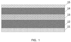
- A photodiode structure comprising a first electrode made of a transparent conductive material at the bottom and a metal electrode at the top, or vice versa, depending on the incident light direction, with an electron transport layer, a light conversion layer made of amorphous silicon, and a hole transport layer, optimized for increased light absorption by selecting materials like molybdenum oxide and zinc oxide, and adjusting thicknesses to enhance light absorption and photoelectric conversion.
Display device and active matrix substrate
PatentWO2010058636A1
Innovation
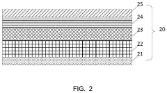
- Incorporating a first shield electrode between the photosensor and pixel electrode, insulated from the pixel electrode, to block electrical noise and prevent light leakage, with the shield electrode being transparent to maintain transmissive display capabilities and potentially opaque to block infrared light.
Display Integration
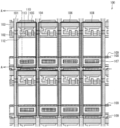
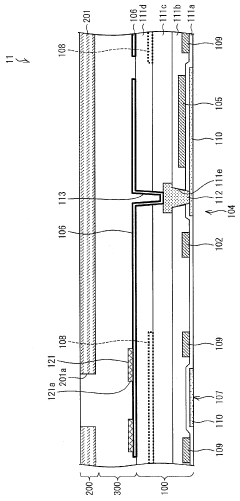
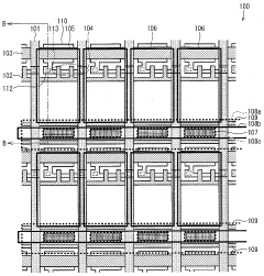
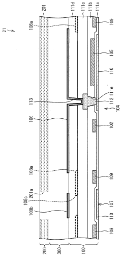
The integration of photodiodes into mobile device displays represents a significant advancement in display technology. This innovation allows for the seamless incorporation of light-sensing capabilities directly within the display panel, enabling a range of new functionalities and improved user experiences.
One of the primary benefits of integrating photodiodes into displays is the ability to achieve more accurate and responsive ambient light sensing. By embedding light sensors throughout the display, devices can more precisely adjust screen brightness to match environmental conditions. This results in improved readability across various lighting scenarios and contributes to enhanced power efficiency by optimizing display illumination.
The integration process involves carefully positioning photodiodes within the display stack, typically between the TFT (Thin-Film Transistor) layer and the color filter layer. This placement allows the photodiodes to capture light that passes through the display, providing valuable data on both ambient light conditions and user interactions. The challenge lies in maintaining display quality while incorporating these additional components, requiring advanced manufacturing techniques and materials.
Another key application of integrated photodiodes is in-display fingerprint sensing. By utilizing an array of photodiodes beneath the display surface, devices can capture high-resolution images of a user's fingerprint when placed on the screen. This technology enables secure biometric authentication without the need for a separate fingerprint sensor, maximizing screen real estate and streamlining device design.
The integration of photodiodes also opens up possibilities for novel user interface interactions. For example, displays can detect hand gestures or object proximity, allowing for touchless control and adaptive user experiences. This capability is particularly valuable in scenarios where physical contact with the device may be impractical or undesirable.
As display technologies continue to evolve, the role of integrated photodiodes is likely to expand. Future developments may include more sophisticated light-sensing arrays capable of capturing detailed spectral information, enabling applications such as on-device color calibration or even basic spectroscopy for material analysis. The ongoing miniaturization of photodiode components will further facilitate their integration into displays without compromising on pixel density or overall device thickness.
Power Efficiency
Power efficiency is a critical aspect of photodiode developments in mobile device displays. As mobile devices continue to evolve, the demand for longer battery life and reduced power consumption has become paramount. In the context of photodiode integration, significant strides have been made to enhance power efficiency without compromising display performance.
One of the key advancements in power efficiency lies in the optimization of photodiode design. Manufacturers have focused on reducing the dark current of photodiodes, which is the small electric current that flows through the device even when no photons are entering it. By minimizing dark current, the overall power consumption of the display system is reduced, leading to improved battery life.
Another area of improvement is the implementation of advanced power management techniques. Modern photodiodes in mobile displays often incorporate intelligent power-saving modes that adjust sensitivity based on ambient light conditions. This adaptive approach ensures that the photodiodes consume only the necessary power for optimal performance, further enhancing overall efficiency.
The integration of low-power readout circuits has also contributed significantly to power efficiency. These circuits are designed to amplify and process the signals from photodiodes while consuming minimal energy. By optimizing the signal chain, manufacturers have been able to reduce the power requirements of the entire display system.
Furthermore, advancements in semiconductor materials and fabrication processes have led to the development of more energy-efficient photodiodes. Novel materials with improved quantum efficiency and lower operating voltages have been introduced, allowing for better light detection with reduced power consumption.
The use of multi-junction photodiodes has emerged as another power-saving strategy. These devices consist of multiple p-n junctions stacked vertically, enabling them to capture a broader spectrum of light more efficiently. This design not only improves the overall sensitivity of the photodiode but also reduces the power needed for effective light detection across various wavelengths.
In recent years, the integration of photodiodes with organic light-emitting diode (OLED) displays has opened new avenues for power efficiency. OLED displays inherently consume less power than traditional LCD screens, and when combined with optimized photodiodes, they offer a synergistic approach to reducing overall device power consumption.
As mobile devices continue to evolve, the focus on power efficiency in photodiode developments remains a top priority. Ongoing research aims to further reduce power consumption while enhancing sensitivity and response times, paving the way for more energy-efficient and capable mobile displays in the future.
Unlock deeper insights with Patsnap Eureka Quick Research — get a full tech report to explore trends and direct your research. Try now!
Generate Your Research Report Instantly with AI Agent
Supercharge your innovation with Patsnap Eureka AI Agent Platform!