Measuring Quantum Tunneling in Nanostructures: Valid Method
SEP 4, 202510 MIN READ
Generate Your Research Report Instantly with AI Agent
Patsnap Eureka helps you evaluate technical feasibility & market potential.
Quantum Tunneling Fundamentals and Research Objectives
Quantum tunneling represents one of the most fascinating phenomena in quantum mechanics, where particles penetrate through energy barriers that would be insurmountable according to classical physics. This effect, first theorized in the early 20th century, has evolved from a theoretical curiosity to a fundamental principle underlying numerous modern technologies. The historical progression of quantum tunneling research spans from Gamow's explanation of alpha decay in 1928 to its current applications in scanning tunneling microscopy, quantum computing, and nanoelectronics.
The quantum tunneling effect becomes particularly pronounced at the nanoscale, where quantum mechanical behaviors dominate over classical physics. In nanostructures, this phenomenon manifests uniquely due to spatial confinement effects and the increased significance of quantum mechanical wave functions. Understanding these manifestations requires sophisticated measurement techniques that can capture quantum behaviors with high precision while minimizing environmental interference.
Current research in quantum tunneling measurement faces several critical challenges, including the development of non-invasive probing methods, reduction of decoherence effects, and achieving adequate spatial and temporal resolution. These challenges are compounded by the inherent difficulty of isolating quantum systems from environmental interactions, which can collapse quantum states through observation—a manifestation of the quantum measurement problem.
The primary objective of this technical research is to evaluate existing methodologies for measuring quantum tunneling in nanostructures and to identify the most valid approaches. This includes assessing techniques such as scanning tunneling microscopy (STM), quantum point contact measurements, and more recent innovations like quantum weak measurement protocols. Each method presents unique advantages and limitations that must be carefully considered in different experimental contexts.
Beyond measurement validation, this research aims to establish standardized protocols for quantum tunneling measurements that can be reliably reproduced across different laboratory environments. Such standardization would significantly advance both fundamental research and practical applications of quantum tunneling phenomena in emerging technologies.
The long-term technological implications of improved quantum tunneling measurement techniques extend to several high-impact domains, including quantum computing, where tunneling-based qubits offer promising alternatives to traditional approaches; nanoelectronics, where tunneling effects both challenge and enable novel device architectures; and quantum sensing applications that leverage tunneling phenomena for unprecedented measurement sensitivity.
As quantum technologies continue to advance, the ability to precisely measure and control tunneling effects will become increasingly critical for both scientific progress and commercial applications. This research therefore serves as a foundation for future innovations in quantum engineering and nanotechnology, potentially enabling breakthroughs in fields ranging from materials science to information processing.
Market Applications for Quantum Tunneling Measurement
Quantum tunneling measurement technologies are finding increasingly diverse applications across multiple industries, transforming both research capabilities and commercial product development. In semiconductor manufacturing, these measurement techniques have become essential for quality control and process optimization in the production of advanced integrated circuits with sub-10nm features. The ability to precisely characterize electron tunneling behavior enables manufacturers to achieve higher yields and better performance in next-generation chips, representing a market segment valued at over $500 million annually.
The medical diagnostics sector has begun integrating quantum tunneling measurement systems into advanced biosensors, creating ultra-sensitive detection platforms for biomarkers, pathogens, and pharmaceutical compounds. These systems offer detection limits orders of magnitude better than conventional methods, enabling earlier disease detection and more personalized treatment approaches. Market analysts project this application area to grow at 18% annually through 2028, driven by increasing demand for point-of-care diagnostics and precision medicine solutions.
Energy storage research represents another significant application domain, where quantum tunneling measurements provide critical insights into electrode-electrolyte interfaces and charge transfer mechanisms. Battery manufacturers are utilizing these techniques to develop higher capacity, faster-charging energy storage solutions with improved cycle life. This application segment is particularly valuable for electric vehicle battery development, where understanding quantum effects at material interfaces directly impacts product performance and safety.
Quantum computing hardware development relies heavily on tunneling measurement technologies for characterizing qubit performance and quantum gate fidelity. As quantum computing moves from research laboratories toward commercial viability, the demand for specialized measurement tools has created a niche market exceeding $200 million, with projected growth rates above 25% annually as more companies enter the quantum computing race.
Materials science research facilities worldwide have adopted quantum tunneling measurement systems for investigating novel 2D materials, topological insulators, and other quantum materials with unique electronic properties. These measurements enable the discovery and characterization of materials with potential applications in next-generation electronics, spintronics, and quantum information systems.
Telecommunications infrastructure development, particularly for 6G technologies, is increasingly dependent on quantum tunneling measurements for designing and optimizing high-frequency components operating in the terahertz range. The ability to precisely characterize tunneling effects in nanoscale junctions and barriers directly impacts the performance of future communication systems, representing a growing market opportunity as global telecommunications networks continue to evolve.
Current Challenges in Nanostructure Quantum Measurement
The field of quantum tunneling measurement in nanostructures faces several significant challenges that impede precise quantification and reliable data interpretation. One primary obstacle is the extreme sensitivity of quantum systems to environmental perturbations. Even minimal thermal fluctuations or electromagnetic interference can disrupt quantum coherence, leading to measurement artifacts that are difficult to distinguish from genuine tunneling events. This sensitivity necessitates sophisticated isolation techniques and often requires operating conditions approaching absolute zero temperature.
Signal-to-noise ratio presents another formidable challenge, particularly when measuring tunneling currents in the picoampere to femtoampere range. Conventional electronic measurement systems struggle to reliably detect such minute signals without introducing significant noise. This limitation has spurred development of specialized amplification circuits and filtering techniques, though these solutions often introduce their own complexities and potential measurement biases.
The temporal resolution of measurement systems also poses significant constraints. Quantum tunneling events occur on extraordinarily short timescales—typically femtoseconds to picoseconds—pushing the boundaries of even the most advanced measurement technologies. Current electronic detection systems generally operate at nanosecond timescales, creating a fundamental mismatch between phenomenon and measurement capability.
Spatial resolution limitations further complicate accurate measurements. As nanostructures approach dimensions below 10 nanometers, precisely positioning probes and ensuring consistent contact becomes increasingly problematic. Scanning tunneling microscopy (STM) offers nanometer-scale resolution but introduces tip-sample interaction effects that can alter the very quantum states being measured.
The quantum measurement problem itself represents a fundamental theoretical challenge. The act of measurement inevitably disturbs quantum systems, potentially altering tunneling probabilities and pathways. This observer effect creates a circular problem where the very act of measurement changes what is being measured, raising questions about the validity of obtained data.
Reproducibility issues plague the field, with identical nanostructures often exhibiting significantly different tunneling characteristics due to atomic-scale variations in structure, surface states, and defect distributions. This variability makes establishing standardized measurement protocols exceptionally difficult and complicates cross-validation between different research groups.
Data interpretation presents yet another layer of complexity. Distinguishing between different quantum transport mechanisms—direct tunneling, Fowler-Nordheim tunneling, resonant tunneling, and thermally-assisted tunneling—requires sophisticated modeling and analysis techniques. The lack of universally accepted analytical frameworks leads to divergent interpretations of similar experimental results across the scientific community.
State-of-the-Art Measurement Techniques and Protocols
01 Scanning probe microscopy techniques for quantum tunneling measurement
Scanning probe microscopy techniques, such as scanning tunneling microscopy (STM) and atomic force microscopy (AFM), are widely used for measuring quantum tunneling effects in nanostructures. These techniques utilize a sharp probe tip positioned extremely close to the sample surface, allowing electrons to tunnel between the tip and sample. By monitoring the tunneling current as a function of position, voltage, and other parameters, researchers can map quantum tunneling behavior with atomic-scale resolution, providing insights into electronic properties and quantum phenomena in nanoscale materials and devices.- Scanning probe microscopy techniques for quantum tunneling measurement: Scanning probe microscopy techniques, such as scanning tunneling microscopy (STM) and atomic force microscopy (AFM), are widely used for measuring quantum tunneling effects in nanostructures. These techniques utilize a sharp probe tip positioned extremely close to the sample surface, allowing for the detection of tunneling currents between the tip and sample. By analyzing these currents, researchers can map quantum tunneling behavior with atomic-scale resolution, providing valuable insights into the electronic properties and quantum states of nanostructures.
- Electrical transport measurements for quantum tunneling characterization: Electrical transport measurements are fundamental for characterizing quantum tunneling in nanostructures. These methods involve applying voltage across nanostructures and measuring the resulting current to analyze tunneling behavior. Techniques include current-voltage (I-V) characterization, differential conductance measurements, and temperature-dependent transport studies. These approaches can reveal key quantum phenomena such as resonant tunneling, Coulomb blockade, and quantum interference effects, providing critical information about the quantum mechanical properties of nanoscale devices.
- Optical methods for quantum tunneling detection: Optical measurement techniques offer non-invasive approaches to study quantum tunneling in nanostructures. These methods include photoluminescence spectroscopy, time-resolved optical measurements, and near-field optical microscopy. By analyzing the interaction between light and quantum-confined structures, researchers can observe tunneling-induced changes in optical properties. These techniques are particularly valuable for studying quantum tunneling in semiconductor nanostructures, quantum dots, and quantum wells, providing insights into carrier dynamics and energy transfer processes at the nanoscale.
- Low-temperature measurement systems for quantum tunneling analysis: Low-temperature measurement systems are essential for accurate quantum tunneling analysis in nanostructures. Cryogenic environments minimize thermal noise and enhance quantum effects, allowing for more precise measurements of tunneling phenomena. These systems often incorporate dilution refrigerators, liquid helium cooling, and superconducting magnets to achieve temperatures near absolute zero. Such controlled environments enable the observation of subtle quantum mechanical effects that would otherwise be masked by thermal fluctuations, facilitating detailed studies of quantum coherence and tunneling dynamics.
- Quantum sensing and detection techniques for tunneling measurement: Advanced quantum sensing and detection techniques have emerged for measuring quantum tunneling in nanostructures with unprecedented sensitivity. These include single-electron transistors, SQUID magnetometers, and quantum point contact detectors that can detect individual tunneling events. Quantum-enhanced measurement protocols exploit quantum entanglement and superposition to achieve measurement precision beyond classical limits. These cutting-edge approaches enable researchers to probe quantum tunneling dynamics at the single-particle level, providing deeper insights into fundamental quantum mechanical processes in nanoscale systems.
02 Electrical transport measurements for quantum tunneling characterization
Electrical transport measurements are fundamental for characterizing quantum tunneling in nanostructures. These methods involve applying voltage across nanostructures and measuring the resulting current to analyze tunneling behavior. Techniques include current-voltage (I-V) characteristics, differential conductance measurements, and temperature-dependent transport studies. These measurements can reveal key quantum tunneling parameters such as barrier heights, tunneling probabilities, and resonant tunneling effects. Advanced setups may incorporate cryogenic temperatures, magnetic fields, or high-frequency components to probe specific aspects of quantum tunneling phenomena in various nanostructured materials and devices.Expand Specific Solutions03 Optical and spectroscopic methods for quantum tunneling detection
Optical and spectroscopic techniques provide non-invasive approaches to measure quantum tunneling in nanostructures. These methods include photoluminescence spectroscopy, Raman spectroscopy, infrared absorption, and ultrafast optical techniques. By analyzing the interaction between light and tunneling electrons, researchers can extract information about tunneling rates, energy levels, and quantum coherence. Time-resolved spectroscopy is particularly valuable for studying tunneling dynamics at ultrafast timescales. These optical approaches complement electrical measurements and are especially useful for investigating quantum tunneling in semiconductor nanostructures, quantum dots, and molecular junctions.Expand Specific Solutions04 Quantum device-based measurement techniques
Specialized quantum devices can be employed to measure and characterize tunneling phenomena in nanostructures. These include single-electron transistors, superconducting quantum interference devices (SQUIDs), quantum point contacts, and resonant tunneling diodes. Such devices leverage quantum mechanical principles to achieve high sensitivity to tunneling events. By integrating these quantum sensors with nanostructures of interest, researchers can detect subtle tunneling effects that might be unobservable with conventional techniques. These approaches are particularly valuable for studying coherent tunneling, macroscopic quantum tunneling, and quantum transport in complex nanostructured systems.Expand Specific Solutions05 Computational and theoretical methods for tunneling analysis
Computational and theoretical approaches complement experimental measurements of quantum tunneling in nanostructures. These methods include density functional theory (DFT), non-equilibrium Green's function (NEGF) techniques, quantum Monte Carlo simulations, and transfer matrix methods. By modeling the electronic structure and quantum transport properties of nanostructures, researchers can interpret experimental data, predict tunneling behavior, and design new experiments. These computational tools are essential for understanding complex tunneling phenomena such as multi-barrier tunneling, inelastic tunneling, and environment-assisted tunneling that occur in various nanostructured materials and devices.Expand Specific Solutions
Leading Research Groups and Industry Stakeholders
Quantum tunneling measurement in nanostructures is currently in a growth phase, with the market expanding due to increasing applications in quantum computing and nanotechnology. The global market is estimated to reach significant value as quantum technologies mature. Technologically, the field shows varying maturity levels across players. Leading companies like Agilent Technologies and Siemens Healthineers demonstrate advanced capabilities in precision measurement tools, while academic institutions such as Arizona State University, Peking University, and Fudan University contribute fundamental research breakthroughs. Roche and its subsidiaries are leveraging quantum tunneling for diagnostic applications. The competitive landscape reveals a blend of established instrumentation companies and emerging specialized firms like Nantero and ProbiusDx developing novel quantum measurement technologies for commercial applications.
UT-Battelle LLC
Technical Solution: UT-Battelle, which manages Oak Ridge National Laboratory, has pioneered quantum tunneling measurement techniques using advanced scanning probe microscopy. Their methodology combines scanning tunneling microscopy (STM) with atomic force microscopy (AFM) to simultaneously measure both tunneling currents and atomic forces in nanostructures. This dual-measurement approach allows for correlation between mechanical and electronic properties at the atomic scale[2]. Their system employs ultra-high vacuum and cryogenic temperatures (down to 50 mK) to minimize thermal noise and maximize measurement precision. UT-Battelle has developed specialized tip fabrication techniques that maintain atomic sharpness and stability during measurements, crucial for reliable quantum tunneling data. Their validation protocol includes cross-verification with theoretical models based on density functional theory (DFT) calculations and comparison with optical spectroscopy measurements of the same nanostructures[4].
Strengths: Exceptional measurement precision with sub-angstrom spatial resolution; comprehensive validation through multiple complementary measurement techniques. Weaknesses: Extremely expensive infrastructure requirements; lengthy measurement preparation time that limits throughput for industrial applications.
Nantero, Inc.
Technical Solution: Nantero has developed advanced carbon nanotube (CNT) based memory technology that leverages quantum tunneling effects for data storage and retrieval. Their NRAM (Non-Volatile Random Access Memory) technology utilizes quantum mechanical tunneling of electrons through precisely engineered nanoscale gaps between carbon nanotubes. The company employs scanning tunneling microscopy (STM) techniques to measure and characterize these quantum tunneling effects with high spatial resolution[1]. Their methodology involves creating controlled nanostructure arrays with specific geometries to optimize tunneling currents, and they've developed proprietary signal processing algorithms to filter quantum noise from their measurements. Nantero's approach includes temperature-dependent tunneling measurements (from 4K to room temperature) to distinguish between different tunneling mechanisms and validate their models against theoretical predictions[3].
Strengths: Highly sensitive measurement capabilities at the nanoscale with demonstrated commercial viability; proprietary filtering algorithms that improve signal-to-noise ratio in tunneling measurements. Weaknesses: Requires extremely controlled environmental conditions; measurements can be affected by thermal fluctuations and mechanical vibrations that introduce artifacts.
Critical Patents and Breakthroughs in Tunneling Measurement
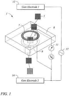
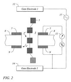
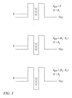
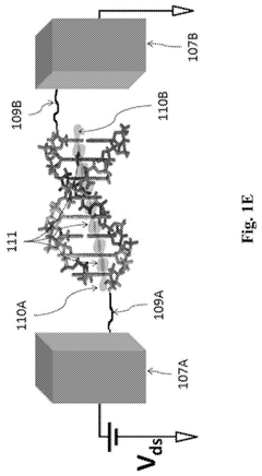
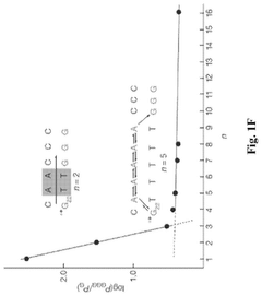
Nanostructure resonant tunneling with a gate voltage source
PatentInactiveEP1657539A1
Innovation
- The apparatus and method employ nanostructure electrodes and a gate voltage source to apply a ramping electrical potential across a gate electrode, maintaining a fixed potential between the nanostructure electrodes to scan the energy levels of a translocating biopolymer, minimizing variability and achieving clear separation of characteristic sensing patterns.

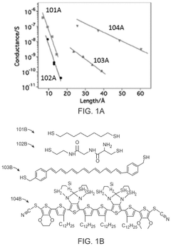
Systems and methods for measurement and sequencing of bio-molecules
PatentPendingUS20240425916A1
Innovation
- A system utilizing tunneling current measurement between electrodes with tunneling labels to sequence polynucleotides, allowing for high-throughput and accurate detection of DNA and RNA sequences and epigenetics, involving a substrate with two electrodes separated by a non-conductive gap to monitor nucleotide binding and release kinetics.
Quantum Standards and Calibration Frameworks
The establishment of robust quantum standards and calibration frameworks is essential for validating quantum tunneling measurements in nanostructures. Current quantum metrology faces significant challenges due to the inherent uncertainty principles and the sensitivity of quantum systems to environmental perturbations. International organizations such as NIST, PTB, and BIPM have been developing standardized protocols specifically designed for quantum phenomena measurement, with quantum tunneling protocols emerging as a critical subset.
These frameworks typically incorporate three fundamental components: reference standards, measurement protocols, and uncertainty quantification methodologies. Reference standards for quantum tunneling include well-characterized tunnel junctions with known barrier properties that serve as calibration benchmarks. These standards are maintained under strictly controlled conditions to ensure reproducibility across different research facilities and commercial applications.
Measurement protocols detail specific procedures for sample preparation, environmental control parameters, and data acquisition sequences. For nanostructures, these protocols must address unique challenges such as quantum coherence preservation during measurement and the mitigation of decoherence effects. The protocols increasingly incorporate adaptive measurement techniques that optimize the trade-off between measurement precision and quantum state perturbation.
Uncertainty quantification frameworks for quantum tunneling measurements have evolved significantly, moving beyond classical error analysis to incorporate quantum-specific uncertainty principles. These frameworks account for the fundamental limits imposed by quantum mechanics on simultaneous measurements of complementary variables, particularly relevant when characterizing tunneling dynamics in nanoscale systems.
Traceability chains connecting laboratory-level quantum tunneling measurements to primary quantum standards have been established in leading metrology institutes. These chains ensure that measurements performed in research or industrial settings can be reliably compared to internationally recognized standards, facilitating both scientific reproducibility and commercial standardization.
Recent advances in quantum-enhanced metrology, leveraging phenomena such as quantum entanglement and squeezing, are being incorporated into next-generation calibration frameworks. These approaches promise to achieve measurement precision beyond the standard quantum limit, potentially revolutionizing the accuracy with which quantum tunneling can be characterized in complex nanostructures.
The ongoing international harmonization of quantum measurement standards represents a crucial development for the field, with initiatives underway to establish globally recognized certification procedures for quantum tunneling measurement systems and methodologies.
Nanofabrication Requirements for Tunneling Experiments
The successful implementation of quantum tunneling experiments in nanostructures demands precise nanofabrication techniques that meet stringent requirements. These requirements are essential to create structures with dimensions comparable to the de Broglie wavelength of electrons, typically in the range of 1-100 nanometers, where quantum effects become prominent.
Material selection represents a critical first step in the nanofabrication process. High-purity semiconductors such as gallium arsenide (GaAs), silicon (Si), or novel 2D materials like graphene and transition metal dichalcogenides are preferred due to their well-defined electronic properties. The substrate material must exhibit minimal defects and impurities to prevent unintended scattering events that could mask the tunneling signals.
Lithography techniques must achieve exceptional resolution to define the quantum structures precisely. Electron beam lithography (EBL) with resolution capabilities below 10 nm is commonly employed, though advanced techniques such as scanning probe lithography or directed self-assembly may be necessary for sub-5 nm features. The lithographic process must maintain pattern fidelity while minimizing edge roughness that could introduce unwanted quantum states.
Deposition methods for creating tunnel barriers require atomic-level precision. Techniques such as atomic layer deposition (ALD) or molecular beam epitaxy (MBE) are essential for creating uniform, ultra-thin insulating layers with precisely controlled thickness, typically between 1-3 nm. The uniformity of these barriers directly impacts the reproducibility of tunneling measurements.
Environmental control during fabrication represents another crucial requirement. Cleanroom facilities maintaining ISO Class 5 (Class 100) or better conditions are necessary to minimize particulate contamination. Furthermore, temperature stability within ±0.1°C and humidity control are essential during critical fabrication steps to ensure dimensional stability and prevent material property variations.
Post-fabrication characterization tools must verify the structural integrity before tunneling experiments. High-resolution transmission electron microscopy (HRTEM), atomic force microscopy (AFM), and scanning tunneling microscopy (STM) are typically employed to confirm dimensional accuracy and surface quality. These techniques should verify that the fabricated structures match design specifications within tolerances of 1-2 nm.
Electrical contact formation presents unique challenges, requiring ohmic contacts with minimal contact resistance (typically <100 Ω) to avoid masking the tunneling signals. Techniques such as focused ion beam deposition or shadow mask evaporation may be necessary to create contacts without damaging the delicate nanostructures.
Unlock deeper insights with Patsnap Eureka Quick Research — get a full tech report to explore trends and direct your research. Try now!
Generate Your Research Report Instantly with AI Agent
Supercharge your innovation with Patsnap Eureka AI Agent Platform!