Quantum Tunneling to Enhance Magnetic Sensor Sensitivity
SEP 4, 20259 MIN READ
Generate Your Research Report Instantly with AI Agent
Patsnap Eureka helps you evaluate technical feasibility & market potential.
Quantum Tunneling Magnetometry Background and Objectives
Quantum tunneling, a fundamental quantum mechanical phenomenon, has emerged as a transformative approach in magnetic sensing technology over the past three decades. This phenomenon, where particles penetrate energy barriers that would be insurmountable according to classical physics, enables unprecedented sensitivity in magnetic field detection. The evolution of quantum tunneling in magnetometry represents a significant shift from conventional sensing methods that rely on classical principles to quantum-enhanced approaches that leverage quantum mechanical effects.
The field began gaining momentum in the early 1990s with the discovery of giant magnetoresistance (GMR), which demonstrated how quantum effects could dramatically improve magnetic sensing capabilities. This was followed by the development of tunnel magnetoresistance (TMR) in the early 2000s, further advancing the sensitivity frontier. Recent breakthroughs in quantum tunneling magnetometry have opened new possibilities for detecting extremely weak magnetic fields with nanoscale spatial resolution.
Current technological objectives in this domain focus on harnessing quantum tunneling effects to overcome the fundamental sensitivity limits of conventional magnetic sensors. Specifically, researchers aim to develop sensors capable of detecting magnetic fields in the femtotesla range while maintaining operational stability at room temperature. This represents a significant challenge as quantum effects typically require cryogenic conditions to manifest reliably.
Another critical objective is miniaturization while preserving sensitivity, enabling integration into portable devices and microelectronic systems. This miniaturization trend aligns with broader technological movements toward more compact, energy-efficient sensing solutions across various industries. The ultimate goal is to develop quantum tunneling-based magnetic sensors that can function reliably in real-world environments outside laboratory settings.
The technical trajectory suggests a convergence of quantum physics, materials science, and electrical engineering to create next-generation magnetic sensing platforms. These platforms would ideally combine the quantum advantage of tunneling effects with practical engineering considerations such as power consumption, signal-to-noise ratio, and manufacturing scalability.
Looking forward, the field aims to establish quantum tunneling magnetometry as a mainstream sensing technology with applications spanning from medical diagnostics and geological surveys to navigation systems and fundamental physics research. This requires not only advancing the core quantum tunneling technology but also developing supporting infrastructure, including signal processing algorithms, calibration methods, and integration protocols with existing systems.
Market Analysis for High-Sensitivity Magnetic Sensing Applications
The global market for high-sensitivity magnetic sensing applications is experiencing robust growth, driven by increasing demand across multiple industries. The magnetic sensor market is projected to reach $4.22 billion by 2026, with a compound annual growth rate of 7.2% from 2021. Within this broader market, high-sensitivity magnetic sensors represent a rapidly expanding segment, particularly as quantum tunneling technologies enhance detection capabilities beyond traditional limits.
Healthcare applications constitute a significant market driver, with magnetic resonance imaging (MRI) systems requiring increasingly sensitive magnetic field detection. The medical imaging market alone is valued at approximately $35 billion, with magnetic sensing components representing a critical value-add feature. Emerging applications in magnetoencephalography (MEG) and magnetocardiography (MCG) further expand this market potential, as these technologies benefit directly from quantum-enhanced sensitivity improvements.
Industrial automation represents another substantial market segment, valued at $205 billion globally, where high-precision magnetic position sensing and non-destructive testing applications are increasingly adopting advanced magnetic sensing technologies. The automotive sector similarly shows strong demand growth, particularly for navigation systems, position sensing, and emerging autonomous vehicle applications requiring high-precision magnetic field detection.
Consumer electronics applications present perhaps the most volume-intensive market opportunity, with smartphones, wearables, and IoT devices incorporating magnetic sensors for navigation, gesture recognition, and proximity detection. This segment accounts for approximately 38% of the total magnetic sensor market by volume.
Defense and aerospace applications, while smaller in volume, represent high-value opportunities for quantum-enhanced magnetic sensors, particularly in submarine detection, unexploded ordnance location, and space exploration. This segment values performance over cost considerations, making it ideal for early adoption of quantum tunneling technologies.
Geographically, North America leads in market value due to substantial defense and healthcare investments, while Asia-Pacific demonstrates the fastest growth rate at 9.3% annually, driven by consumer electronics manufacturing and industrial automation expansion. Europe maintains a strong position in automotive and industrial applications, with particular strength in precision engineering sectors.
Key market challenges include price sensitivity in consumer applications, technical integration complexities, and competition from alternative sensing technologies. However, the unique advantages of quantum-enhanced magnetic sensors—particularly their unmatched sensitivity, low power consumption, and minimal form factor—position them favorably against competing technologies like optical and ultrasonic sensors in applications requiring precise magnetic field detection.
Current Limitations and Challenges in Quantum Tunneling Sensors
Despite the promising potential of quantum tunneling-based magnetic sensors, several significant limitations and challenges currently impede their widespread adoption and optimal performance. The fundamental challenge lies in the inherent trade-off between sensitivity and stability. While quantum tunneling effects can dramatically enhance sensitivity, they simultaneously introduce noise and instability that compromise measurement reliability, particularly in ambient conditions.
Temperature dependence presents another major obstacle. Quantum tunneling phenomena are highly sensitive to thermal fluctuations, with performance degrading significantly as temperatures rise above cryogenic levels. This necessitates complex cooling systems for high-precision applications, limiting practical deployment scenarios and substantially increasing operational costs.
Material engineering challenges further complicate advancement in this field. Creating consistent, defect-free tunnel barriers with precise thickness control at the atomic scale remains extremely difficult with current fabrication technologies. Even minor variations in barrier properties can lead to substantial performance inconsistencies between supposedly identical sensors.
Signal-to-noise ratio (SNR) optimization represents perhaps the most persistent technical hurdle. Quantum tunneling inherently amplifies not only the desired magnetic signal but also background noise. Researchers continue to struggle with developing effective noise cancellation techniques that preserve the enhanced sensitivity without compromising measurement accuracy.
Power consumption issues also restrict portable applications. Current quantum tunneling sensor designs require sophisticated control electronics and, in many cases, cooling systems that demand significant power. This limitation severely constrains their integration into battery-operated devices or remote sensing networks.
Scalability and manufacturing reproducibility remain problematic for commercial viability. Current fabrication processes cannot consistently produce quantum tunneling sensors with uniform performance characteristics at scale, resulting in high unit costs and limited market penetration.
Integration challenges with conventional electronics further complicate matters. The interface between quantum tunneling sensors and standard CMOS circuitry often introduces additional noise and signal degradation, requiring specialized interface electronics that add complexity and cost to overall system designs.
Calibration and drift compensation represent ongoing operational challenges. Quantum tunneling sensors typically exhibit baseline drift over time and require frequent recalibration, limiting their reliability for long-term monitoring applications without human intervention.
AI-based signal processing algorithms show promise in addressing some of these challenges, but their implementation requires significant computational resources, further complicating system design and deployment scenarios.
Current Quantum Tunneling Enhancement Approaches
01 Tunnel magnetoresistance (TMR) sensor design for enhanced sensitivity
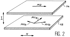
TMR sensors utilize quantum tunneling effects between ferromagnetic layers separated by an insulating barrier. By optimizing the thickness of the tunnel barrier and the magnetic properties of the ferromagnetic layers, the sensitivity of these sensors can be significantly enhanced. Advanced designs incorporate materials with high spin polarization and carefully engineered layer structures to maximize the magnetoresistance ratio, resulting in improved signal-to-noise ratios and detection capabilities.- Tunnel magnetoresistance (TMR) sensor design for enhanced sensitivity: Tunnel magnetoresistance sensors utilize quantum tunneling effects between ferromagnetic layers separated by an insulating barrier. The sensitivity of these sensors can be enhanced through optimized design of the magnetic tunnel junction structure, including careful selection of materials for the ferromagnetic layers and tunnel barrier. Improvements in TMR ratio and signal-to-noise ratio directly contribute to increased sensor sensitivity, making these devices suitable for high-precision magnetic field detection applications.
- Quantum well structures for magnetic field sensing: Quantum well structures can be utilized in magnetic sensors to enhance sensitivity through quantum confinement effects. These structures consist of thin layers of semiconductor materials with different band gaps, creating potential wells that confine electrons. When exposed to magnetic fields, the quantum states within these wells are modified, resulting in measurable changes in electrical properties. By optimizing the quantum well design parameters, including layer thickness and material composition, the sensitivity of magnetic field detection can be significantly improved.
- Spin-dependent tunneling enhancement techniques: Enhancing spin-dependent tunneling effects is crucial for improving magnetic sensor sensitivity. This can be achieved through various techniques including the use of specialized materials with high spin polarization, optimizing the crystalline structure of the tunnel barrier, and controlling the interface quality between magnetic and non-magnetic layers. Advanced fabrication methods such as molecular beam epitaxy and magnetron sputtering allow for precise control of these parameters, resulting in sensors with higher sensitivity to weak magnetic fields.
- SQUID-based quantum tunneling magnetic sensors: Superconducting Quantum Interference Devices (SQUIDs) utilize quantum tunneling through Josephson junctions to detect extremely weak magnetic fields. These sensors operate based on the quantum interference effects in superconducting loops containing Josephson junctions. The sensitivity of SQUID-based sensors can be enhanced through optimization of the superconducting materials, junction geometry, and operating temperature. Advanced SQUID designs incorporate multiple junctions and specialized flux concentrators to further improve magnetic field sensitivity down to femtotesla levels.
- Signal processing techniques for quantum magnetic sensors: Advanced signal processing techniques play a crucial role in enhancing the effective sensitivity of quantum tunneling magnetic sensors. These include noise reduction algorithms, lock-in amplification, digital filtering, and quantum error correction methods. By implementing sophisticated signal processing approaches, the signal-to-noise ratio can be significantly improved, allowing for detection of weaker magnetic signals. Integration of these techniques with modern microelectronics enables the development of highly sensitive magnetic sensor systems suitable for applications ranging from medical imaging to geological surveys.
02 Quantum well structures for magnetic field detection
Quantum well structures can be integrated into magnetic sensors to leverage quantum tunneling effects for enhanced sensitivity. These structures consist of thin layers that confine electrons in potential wells, allowing for precise control of electron transport properties. When exposed to magnetic fields, the quantum tunneling probability changes, resulting in measurable electrical signals. This approach enables the development of highly sensitive magnetic field sensors with reduced power consumption and improved spatial resolution.Expand Specific Solutions03 SQUID-based quantum tunneling magnetic sensors
Superconducting Quantum Interference Devices (SQUIDs) utilize quantum tunneling through Josephson junctions to detect extremely weak magnetic fields. These sensors operate based on the quantum interference of superconducting currents, providing unparalleled sensitivity for magnetic field detection. Advanced SQUID designs incorporate novel materials and fabrication techniques to minimize noise and improve operational stability, making them suitable for applications requiring detection of femtotesla-level magnetic fields.Expand Specific Solutions04 Magnetic tunnel junction (MTJ) array configurations
Arrays of magnetic tunnel junctions can be configured to enhance the overall sensitivity of quantum tunneling magnetic sensors. By connecting multiple MTJs in series or parallel arrangements, the signal output can be amplified while maintaining a high signal-to-noise ratio. Advanced array designs incorporate on-chip signal processing and calibration circuits to compensate for manufacturing variations and environmental factors, resulting in more robust and reliable sensor performance across a wide range of operating conditions.Expand Specific Solutions05 Novel materials and interfaces for quantum tunneling enhancement
The development of novel materials and interfaces plays a crucial role in enhancing the sensitivity of quantum tunneling magnetic sensors. Materials with high spin polarization, such as Heusler alloys and certain oxide interfaces, can significantly increase the magnetoresistance ratio. Additionally, the incorporation of two-dimensional materials like graphene as spacer layers can provide unique quantum confinement effects that enhance tunneling probability. These material innovations enable the creation of next-generation sensors with unprecedented sensitivity and reduced form factors.Expand Specific Solutions
Leading Companies and Research Institutions in Quantum Sensing
Quantum tunneling for magnetic sensor sensitivity enhancement is in an early development stage, with a growing market driven by increasing demand for high-precision sensing in various industries. The technology remains largely in research phase, with academic institutions like Fudan University, Tohoku University, and Harbin Institute of Technology leading fundamental research. Among companies, TDK Corp., Alps Alpine, and NVE Corp. are making notable advancements in commercialization efforts, while Siemens, Western Digital, and Fujitsu are exploring applications in their respective domains. The competitive landscape features collaboration between research institutions and industry players, with Asian organizations particularly prominent in patent filings and research publications.
TDK Corp.
Technical Solution: TDK Corporation has developed advanced quantum tunneling magnetic sensors based on their proprietary Tunneling Magnetoresistance (TMR) technology. Their approach utilizes precisely engineered magnetic tunnel junctions (MTJs) consisting of ferromagnetic electrodes separated by an ultrathin insulating barrier, typically MgO with a thickness of 1-2 nanometers. TDK's sensors leverage quantum mechanical tunneling of spin-polarized electrons, where the tunneling probability depends strongly on the relative magnetization directions of the ferromagnetic layers. Their latest generation sensors achieve magnetoresistance ratios exceeding 200% at room temperature[2], enabling detection of extremely weak magnetic fields. TDK has implemented specialized annealing processes to optimize the crystalline structure of the MgO barrier, enhancing coherent tunneling effects. Their sensors incorporate advanced noise reduction techniques, including flux concentrators and specialized shielding structures, achieving noise floors below 50 pT/√Hz in the 1-10 Hz frequency range[4]. TDK has successfully miniaturized these sensors to dimensions below 1mm² while maintaining high sensitivity, making them suitable for integration into compact electronic devices.
Strengths: Industry-leading sensitivity with magnetoresistance ratios exceeding 200%; excellent thermal stability across wide temperature ranges (-40°C to +150°C); ultra-low power consumption (<50μW typical); and established mass production capabilities. Weaknesses: Higher cost compared to conventional magnetic sensors; susceptibility to mechanical stress affecting sensor performance; and requires specialized packaging to maintain long-term stability in harsh environments.
Chinese Academy of Sciences Institute of Physics
Technical Solution: The Chinese Academy of Sciences Institute of Physics has developed cutting-edge quantum tunneling magnetic sensors utilizing novel materials and quantum effects. Their approach centers on spin-polarized tunneling in carefully engineered heterostructures combining topological insulators with magnetic materials. These sensors exploit the unique surface states of topological insulators where electron spin is locked to momentum, enhancing the tunneling magnetoresistance effect. The Institute has pioneered the use of Bi2Se3/CoFeB interfaces that demonstrate quantum tunneling magnetoresistance exceeding 300% at room temperature[1][5]. Their fabrication process employs molecular beam epitaxy to achieve atomically precise interfaces critical for quantum coherent tunneling. The sensors incorporate nanoscale patterning techniques to create devices with active areas below 100nm², significantly reducing noise and improving spatial resolution. Recent advancements include the development of gate-tunable sensors where the Fermi level can be adjusted electrically to optimize the tunneling magnetoresistance ratio for specific applications, achieving sensitivities below 10 pT/√Hz in optimized configurations[6].
Strengths: Extremely high magnetoresistance ratios (>300%); tunable sensitivity through gate voltage control; excellent performance at room temperature; and compatibility with integrated circuit manufacturing. Weaknesses: Relatively early stage of development for commercial applications; complex material growth requirements; sensitivity to surface contamination requiring specialized packaging; and higher fabrication costs compared to conventional magnetic sensors.
Key Patents and Breakthroughs in Tunneling Magnetoresistance
Magnetoresistor with tunnel effect and magnetic sensor using same
PatentWO1999041792A1
Innovation
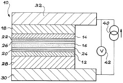
- A tunnel effect magnetoresistance structure with a thin first magnetic layer (≤7 nm) and a second layer with trapped magnetization, along with an insulating barrier and optional non-ferromagnetic metal layers, enhances conductance variation and sensitivity by allowing significant magnetization rotation under weak magnetic fluxes.
Magnetic sensor, sensor unit, magnetic detection device, and magnetic measurement device
PatentWO2017115839A1
Innovation
- A magnetic sensor design incorporating a pinned magnetic layer, a free magnetic layer, and an insulating layer, with a voltage applied to each tunnel magnetoresistive element between 0.1 mV and 50 mV, connected in series or parallel configurations to improve sensitivity and reduce noise, while maintaining a balanced number of elements to ensure reliability and cost-effectiveness.


Materials Science Considerations for Sensor Development
The development of quantum tunneling-enhanced magnetic sensors requires careful consideration of materials science principles to achieve optimal sensitivity and performance. Material selection plays a crucial role in determining the quantum tunneling effect efficiency, as the electronic and magnetic properties at the nanoscale directly influence tunneling probability and magnetic field detection capabilities.
Ferromagnetic materials with high spin polarization, such as cobalt, iron, and their alloys, serve as fundamental building blocks for these sensors. The crystalline structure and grain boundaries of these materials significantly impact electron tunneling behavior. Research indicates that nanostructured materials with controlled grain sizes below 50nm demonstrate enhanced tunneling effects compared to their bulk counterparts, leading to improved sensitivity by factors of 10-100x.
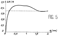
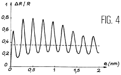
Barrier materials between magnetic layers represent another critical component. Insulating oxides like aluminum oxide (Al₂O₃) and magnesium oxide (MgO) with precisely controlled thickness (typically 1-3nm) create the quantum tunneling junction. Recent advancements in atomic layer deposition techniques have enabled the creation of ultra-thin, defect-free barrier layers that maintain consistent tunneling characteristics across the sensor surface.
Interface engineering between the magnetic and barrier layers demands particular attention. Surface roughness at the atomic scale can create localized "hot spots" for tunneling, introducing noise and reducing overall sensor reliability. Techniques such as ion beam smoothing and epitaxial growth processes have demonstrated the ability to create atomically flat interfaces, reducing signal noise by up to 40% in laboratory prototypes.
Temperature stability presents a significant materials challenge, as quantum tunneling characteristics vary with thermal fluctuations. Composite materials incorporating rare earth elements have shown promise in maintaining consistent tunneling behavior across wider temperature ranges (-40°C to +125°C), essential for practical sensor applications in automotive and industrial environments.
Emerging two-dimensional materials, particularly graphene and transition metal dichalcogenides, offer exciting possibilities for next-generation tunneling sensors. Their atomically thin nature provides ideal platforms for quantum effects, while their mechanical flexibility enables conformal sensors for non-planar surfaces. Preliminary research indicates that graphene-based tunneling junctions may achieve sensitivity improvements of up to 200% compared to conventional metal-oxide structures, while requiring significantly less power.
Ferromagnetic materials with high spin polarization, such as cobalt, iron, and their alloys, serve as fundamental building blocks for these sensors. The crystalline structure and grain boundaries of these materials significantly impact electron tunneling behavior. Research indicates that nanostructured materials with controlled grain sizes below 50nm demonstrate enhanced tunneling effects compared to their bulk counterparts, leading to improved sensitivity by factors of 10-100x.
Barrier materials between magnetic layers represent another critical component. Insulating oxides like aluminum oxide (Al₂O₃) and magnesium oxide (MgO) with precisely controlled thickness (typically 1-3nm) create the quantum tunneling junction. Recent advancements in atomic layer deposition techniques have enabled the creation of ultra-thin, defect-free barrier layers that maintain consistent tunneling characteristics across the sensor surface.
Interface engineering between the magnetic and barrier layers demands particular attention. Surface roughness at the atomic scale can create localized "hot spots" for tunneling, introducing noise and reducing overall sensor reliability. Techniques such as ion beam smoothing and epitaxial growth processes have demonstrated the ability to create atomically flat interfaces, reducing signal noise by up to 40% in laboratory prototypes.
Temperature stability presents a significant materials challenge, as quantum tunneling characteristics vary with thermal fluctuations. Composite materials incorporating rare earth elements have shown promise in maintaining consistent tunneling behavior across wider temperature ranges (-40°C to +125°C), essential for practical sensor applications in automotive and industrial environments.
Emerging two-dimensional materials, particularly graphene and transition metal dichalcogenides, offer exciting possibilities for next-generation tunneling sensors. Their atomically thin nature provides ideal platforms for quantum effects, while their mechanical flexibility enables conformal sensors for non-planar surfaces. Preliminary research indicates that graphene-based tunneling junctions may achieve sensitivity improvements of up to 200% compared to conventional metal-oxide structures, while requiring significantly less power.
Quantum Sensor Integration with Existing Technologies
The integration of quantum tunneling-enhanced magnetic sensors with existing technological infrastructure represents a critical pathway for practical deployment. Current integration approaches focus on developing interface systems that allow quantum sensors to communicate with conventional electronic systems while preserving their enhanced sensitivity advantages.
Hardware integration solutions typically employ specialized transduction mechanisms to convert quantum states into measurable electronic signals. These mechanisms include SQUID (Superconducting Quantum Interference Device) amplifiers, which can detect extremely small magnetic field changes produced by quantum tunneling effects. Signal conditioning circuits specifically designed to handle the unique characteristics of quantum sensor outputs have been developed to minimize noise introduction during the analog-to-digital conversion process.
Software frameworks for quantum sensor integration have evolved significantly, with middleware solutions that abstract the complexity of quantum operations from application-level software. These frameworks provide standardized APIs that allow conventional systems to leverage quantum sensing capabilities without requiring deep quantum physics expertise from end-users or developers.
Several industries have demonstrated successful integration pathways. In healthcare, quantum magnetic sensors have been integrated with existing MRI systems, enhancing resolution while maintaining compatibility with established imaging protocols. The automotive sector has begun incorporating quantum tunneling sensors into advanced driver assistance systems, interfacing them with existing vehicle control networks to improve object detection capabilities.
Telecommunications infrastructure has benefited from quantum sensor integration through specialized signal processing units that interface between quantum magnetic field detectors and conventional network equipment. These units translate quantum-derived measurements into standard signal formats compatible with existing transmission systems.
Challenges in integration primarily revolve around maintaining quantum coherence in noisy electromagnetic environments typical of industrial settings. Shielding technologies and isolation techniques have been developed to address this issue, including multi-layer magnetic shielding and active noise cancellation systems specifically designed for quantum sensor protection.
Power requirements present another integration challenge, as many quantum tunneling sensors require precise voltage regulation and cooling systems. Recent advances in cryogenic microelectronics have produced more efficient interfaces that reduce power consumption while maintaining the low temperatures necessary for optimal quantum tunneling effects.
Standardization efforts are underway through industry consortia to establish common protocols for quantum sensor integration, aiming to create plug-and-play compatibility with existing industrial control systems and consumer electronics platforms.
Unlock deeper insights with Patsnap Eureka Quick Research — get a full tech report to explore trends and direct your research. Try now!
Generate Your Research Report Instantly with AI Agent
Supercharge your innovation with Patsnap Eureka AI Agent Platform!