MicroLED inspection and binning automation to reduce cost per good pixel
AUG 21, 20259 MIN READ
Generate Your Research Report Instantly with AI Agent
Patsnap Eureka helps you evaluate technical feasibility & market potential.
MicroLED Inspection Goals
MicroLED technology has emerged as a promising display solution, offering superior brightness, contrast, and energy efficiency compared to traditional LED and OLED displays. The primary goal of MicroLED inspection and binning automation is to significantly reduce the cost per good pixel, a critical factor in making this technology commercially viable for mass production.
One of the key objectives is to develop high-precision inspection systems capable of detecting defects at the microscopic level. These systems must be able to identify and categorize various types of defects, including dead pixels, color inconsistencies, and structural abnormalities. The inspection process needs to be fast and accurate to keep pace with high-volume production requirements while maintaining stringent quality standards.
Another crucial aim is to implement advanced binning techniques to optimize the yield of usable MicroLED chips. Binning involves sorting LEDs based on their performance characteristics, such as brightness and color, to ensure uniformity in the final display. Automation of this process is essential to handle the vast number of individual MicroLED chips efficiently and consistently.
Reducing human intervention in the inspection and binning processes is a primary goal to minimize labor costs and potential errors. This necessitates the development of sophisticated machine learning algorithms and computer vision systems that can make real-time decisions with high accuracy. These AI-driven systems should be capable of learning and adapting to new defect patterns and production variations over time.
Improving the speed of the inspection and binning processes without compromising accuracy is another critical objective. This involves optimizing the hardware and software components of the automation system to handle the inspection of millions of MicroLEDs in a short time frame. The goal is to achieve throughput rates that align with mass production schedules while maintaining the ability to detect even the smallest defects.
Enhancing the flexibility of the inspection and binning system is also a key aim. The system should be adaptable to different MicroLED sizes, configurations, and production processes. This flexibility will allow manufacturers to use the same automation infrastructure across various product lines, maximizing the return on investment in automation equipment.
Ultimately, the overarching goal of MicroLED inspection and binning automation is to drive down the cost per good pixel to a level that makes MicroLED displays competitive with existing display technologies in terms of price-performance ratio. This involves not only improving the yield of usable pixels but also optimizing the entire production process to reduce waste and increase efficiency. By achieving these goals, the industry aims to accelerate the adoption of MicroLED technology in a wide range of applications, from smartphones and wearables to large-scale displays and automotive systems.
MicroLED Market Analysis
The MicroLED market is experiencing rapid growth and transformation, driven by the technology's potential to revolutionize display applications across various sectors. As demand for high-quality, energy-efficient displays increases, MicroLED technology is positioned to capture a significant market share in the coming years.
The global MicroLED market is projected to expand substantially, with key growth drivers including the rising adoption of MicroLED displays in smartphones, smartwatches, AR/VR devices, and large-scale video walls. The automotive industry is also showing increased interest in MicroLED technology for advanced dashboard displays and infotainment systems.
Consumer electronics remain the largest application segment for MicroLED displays, with smartphones and wearables leading the charge. The superior brightness, contrast ratio, and power efficiency of MicroLED displays make them particularly attractive for these portable devices.
In the large display market, MicroLED technology is gaining traction in high-end televisions and digital signage. The ability to create seamless, bezel-free displays of various sizes and shapes offers unique advantages in these applications.
The automotive sector represents a promising growth area for MicroLED displays. As vehicles become more connected and autonomous, the demand for advanced display technologies in dashboards, heads-up displays, and rear-seat entertainment systems is expected to surge.
Despite the promising outlook, challenges remain in mass production and cost reduction. The inspection and binning process for MicroLED chips is a critical bottleneck, significantly impacting the overall cost per good pixel. Automation of these processes is crucial for improving yield rates and reducing production costs.
Key players in the MicroLED market include established display manufacturers, semiconductor companies, and startups specializing in MicroLED technology. These companies are investing heavily in research and development to overcome technical hurdles and scale up production.
Geographically, Asia-Pacific leads in MicroLED manufacturing, with South Korea, Taiwan, and China at the forefront. North America and Europe are significant contributors to MicroLED research and development, particularly in areas such as chip design and production equipment.
The market dynamics are further influenced by intellectual property considerations, with a complex landscape of patents and licensing agreements shaping industry collaborations and competition. As the technology matures, strategic partnerships and mergers are likely to play a crucial role in market consolidation and technology advancement.
In conclusion, the MicroLED market shows strong growth potential, driven by diverse applications and technological advancements. However, the success of MicroLED technology hinges on overcoming production challenges, particularly in the areas of inspection and binning automation, to achieve cost-effective mass production and wider market adoption.
Challenges in Automation
Automating MicroLED inspection and binning processes presents several significant challenges that need to be addressed to effectively reduce the cost per good pixel. One of the primary obstacles is the development of high-precision, high-speed inspection systems capable of detecting defects at the microscopic level. MicroLEDs are extremely small, often measuring less than 10 micrometers, requiring inspection equipment with exceptional resolution and accuracy.
The sheer volume of MicroLEDs that need to be inspected in a production environment poses another challenge. A single display may contain millions of individual MicroLEDs, necessitating inspection systems that can operate at very high speeds without compromising accuracy. This requirement often leads to a trade-off between throughput and inspection quality, which must be carefully balanced.
Another significant challenge lies in the development of robust and reliable algorithms for defect detection and classification. MicroLEDs can exhibit a wide range of defects, including color variations, brightness inconsistencies, and structural abnormalities. Creating algorithms that can accurately identify and categorize these defects across millions of LEDs is a complex task that requires advanced machine learning and computer vision techniques.
The binning process, which involves sorting MicroLEDs based on their performance characteristics, presents its own set of challenges. Achieving consistent color and brightness across a display requires extremely precise binning. Automating this process while maintaining the necessary level of accuracy is technically demanding and requires sophisticated sorting mechanisms and control systems.
Environmental factors also play a crucial role in the automation challenges. MicroLED production and inspection often need to be conducted in cleanroom environments to prevent contamination. Designing automation systems that can operate reliably in these controlled environments while meeting cleanliness standards adds another layer of complexity to the automation process.
Integrating various automated systems into a cohesive production line presents logistical and technical challenges. Ensuring seamless communication and coordination between inspection, binning, and assembly systems is critical for maintaining efficiency and reducing errors. This integration often requires custom software solutions and robust data management systems to handle the large volumes of information generated during the production process.
Lastly, the rapidly evolving nature of MicroLED technology itself poses a challenge for automation. As new materials, designs, and manufacturing techniques are developed, inspection and binning systems must be flexible enough to adapt to these changes. This requirement for adaptability can complicate the design of automation systems and increase development costs.
Current Inspection Methods
01 Manufacturing process optimization
Improving the manufacturing process for MicroLEDs can significantly reduce the cost per good pixel. This includes developing more efficient transfer and bonding techniques, enhancing yield rates, and implementing automated production lines. Advanced manufacturing methods can help minimize defects and increase overall production efficiency, leading to lower costs.- Manufacturing process optimization: Improving the manufacturing process of MicroLEDs to increase yield and reduce cost per good pixel. This includes developing advanced transfer techniques, enhancing epitaxial growth methods, and implementing precise quality control measures to minimize defects and improve overall production efficiency.
- Novel MicroLED structures: Designing innovative MicroLED structures to improve performance and reduce production costs. This involves developing new pixel architectures, implementing advanced materials, and optimizing the light-emitting layers to enhance efficiency and reduce the number of defective pixels.
- Defect detection and repair techniques: Implementing advanced defect detection and repair methods to increase the yield of good pixels. This includes developing high-resolution inspection systems, utilizing machine learning algorithms for defect identification, and creating innovative repair techniques to salvage defective pixels, thereby reducing overall costs.
- Mass transfer and integration methods: Developing efficient mass transfer and integration techniques for MicroLED production. This involves creating advanced pick-and-place systems, improving alignment accuracy, and optimizing bonding processes to increase throughput and reduce the cost per good pixel in large-scale manufacturing.
- Cost-effective substrate and materials: Exploring and implementing cost-effective substrates and materials for MicroLED production. This includes researching alternative substrate materials, developing more efficient epitaxial growth processes, and optimizing the use of rare earth elements to reduce overall material costs while maintaining or improving pixel quality.
02 Material selection and optimization
Choosing and optimizing materials used in MicroLED production can impact the cost per good pixel. This involves selecting cost-effective substrates, developing improved epitaxial growth techniques, and exploring alternative materials for various components. Optimizing material usage and reducing waste can contribute to overall cost reduction.Expand Specific Solutions03 Defect detection and repair techniques
Implementing advanced defect detection and repair methods can increase the yield of good pixels, thereby reducing the overall cost. This includes developing high-resolution inspection systems, machine learning algorithms for defect identification, and innovative repair techniques such as laser-based pixel correction or redundancy schemes.Expand Specific Solutions04 Scaling and miniaturization
Reducing the size of MicroLEDs while maintaining or improving performance can lead to more efficient use of materials and lower costs. This involves developing advanced lithography techniques, exploring new pixel architectures, and optimizing the overall display design to maximize pixel density while minimizing power consumption and production complexity.Expand Specific Solutions05 Integration and packaging innovations
Improving the integration and packaging processes for MicroLED displays can reduce costs associated with assembly and increase overall yield. This includes developing novel bonding techniques, exploring wafer-level packaging solutions, and optimizing driver circuitry integration. Innovations in this area can lead to more compact and cost-effective MicroLED modules.Expand Specific Solutions
Key Industry Players
The MicroLED inspection and binning automation market is in its growth phase, driven by increasing demand for high-quality displays in various industries. The market size is expanding rapidly, with projections indicating significant growth in the coming years. Technologically, the field is advancing quickly, with companies like Samsung Electronics, LG Display, and Applied Materials leading innovation. These firms are developing sophisticated automation solutions to enhance efficiency and reduce costs in MicroLED production. Emerging players such as eLux and VueReal are also contributing novel approaches to MicroLED manufacturing and inspection processes. The technology's maturity is progressing, but challenges remain in achieving cost-effective mass production, indicating room for further advancements and market expansion.
Samsung Electronics Co., Ltd.
Technical Solution: Samsung has developed an advanced MicroLED inspection and binning automation system that utilizes AI-powered image processing and machine learning algorithms. The system employs high-resolution cameras and spectrophotometers to capture detailed images and spectral data of each MicroLED pixel[1]. Advanced computer vision techniques are used to detect defects, color variations, and brightness inconsistencies with high accuracy. The automation process includes a multi-stage binning system that sorts MicroLEDs based on their performance characteristics, ensuring optimal uniformity in final displays[2]. Samsung's system also incorporates real-time feedback loops to continuously improve inspection accuracy and binning efficiency, resulting in a significant reduction in cost per good pixel[3].
Strengths: High accuracy in defect detection, advanced AI algorithms, and continuous improvement capabilities. Weaknesses: High initial implementation cost and potential over-reliance on proprietary technology.
Applied Materials, Inc.
Technical Solution: Applied Materials has developed a comprehensive MicroLED inspection and binning automation solution that integrates advanced optical inspection technologies with high-speed robotics. Their system utilizes multi-spectral imaging and interferometry to detect sub-micron defects and measure critical dimensions of MicroLEDs[4]. The automation process incorporates a series of high-precision pick-and-place robots that can handle and sort MicroLEDs at speeds exceeding 100,000 units per hour[5]. Applied Materials' solution also features an AI-driven predictive maintenance system that minimizes downtime and optimizes equipment performance, further reducing the cost per good pixel[6].
Strengths: High-speed processing, advanced defect detection capabilities, and integrated predictive maintenance. Weaknesses: Potentially high equipment costs and complexity in system integration.
Innovative Binning Tech
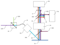
Micro LED Inspection Device for Performing Photoluminescence Inspection and Automatic Optical Inspection Simultaneously
PatentActiveKR1020230068578A
Innovation
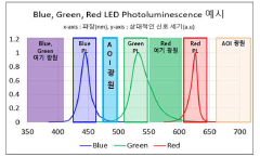
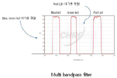
- A micro LED inspection device that simultaneously performs photoluminescence and automatic optical inspections using a photoluminescence light source, automatic optical inspection light source, and optical filters, with specific wavelength configurations and a dichroic mirror to separate and detect scattered and reflected lights.

System and method for the selective harvest of emissive elements
PatentWO2021236552A1
Innovation
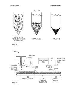
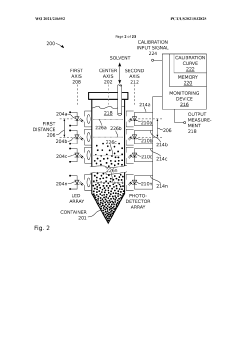
- A selective harvest method and dispensing system are developed to formulate and manipulate microLED suspensions, allowing for the separation of defective LEDs, maintaining adhesive attachment, and ensuring a uniform distribution of functional LEDs on a substrate, using solvent-resistant binding materials and optical measurement techniques to achieve a controlled concentration and dispersion.
Cost Reduction Strategies
Cost reduction strategies for MicroLED inspection and binning automation are crucial for improving the economic viability of this emerging display technology. One primary approach involves optimizing the inspection process through advanced machine vision systems. These systems can rapidly identify defects and categorize LEDs with high accuracy, reducing the need for manual inspection and minimizing human error.
Implementing artificial intelligence and machine learning algorithms can significantly enhance the efficiency of the binning process. These technologies can analyze vast amounts of data to identify patterns and make real-time decisions on LED classification, leading to more precise binning and reduced waste. By automating this process, manufacturers can achieve consistent quality while reducing labor costs and increasing throughput.
Another key strategy is the development of high-speed, multi-parameter testing equipment. Such systems can simultaneously measure multiple characteristics of MicroLEDs, including brightness, color, and uniformity, in a single pass. This approach not only accelerates the inspection process but also provides more comprehensive data for accurate binning, ultimately improving yield and reducing costs.
Integration of in-line inspection and binning processes within the production line can further streamline operations. This eliminates the need for separate handling and transportation steps, reducing the risk of damage to delicate MicroLEDs and minimizing production time. Continuous monitoring and feedback loops can also be implemented to adjust production parameters in real-time, maintaining optimal quality and yield.
Adopting modular and scalable automation solutions allows manufacturers to adapt their processes as technology evolves and production volumes increase. This flexibility ensures that initial investments in automation can be leveraged long-term, spreading costs over larger production runs and enabling economies of scale.
Collaborative robotics and advanced material handling systems can further reduce costs by minimizing physical stress on MicroLEDs during the inspection and binning processes. These systems can handle components with extreme precision, reducing breakage and improving overall yield. Additionally, the use of standardized interfaces and protocols in automation equipment can facilitate easier integration and upgrades, reducing long-term maintenance and upgrade costs.
Quality Control Standards
Quality control standards play a crucial role in the automation of MicroLED inspection and binning processes to reduce the cost per good pixel. These standards ensure consistency, reliability, and efficiency in the production of high-quality MicroLED displays.
One of the primary quality control standards for MicroLED inspection is the measurement of luminance uniformity. This standard involves assessing the brightness consistency across the entire display panel. Automated systems use high-resolution cameras and advanced image processing algorithms to detect variations in luminance, ensuring that each pixel meets the specified brightness thresholds.
Color accuracy is another critical quality control standard in MicroLED production. Automated inspection systems employ spectrophotometers to measure the color coordinates of each pixel, comparing them against predefined color gamut standards. This process helps identify and segregate LEDs that fall outside the acceptable color range, maintaining color consistency across the display.
Defect detection is a fundamental aspect of quality control in MicroLED manufacturing. Automated systems utilize machine vision technologies to identify various types of defects, including dead pixels, shorts, and contamination. These systems are calibrated to detect defects at the microscopic level, ensuring that only LEDs meeting stringent quality criteria proceed to the next production stage.
Binning, an essential process in MicroLED production, relies on precise quality control standards to categorize LEDs based on their performance characteristics. Automated binning systems sort LEDs according to their luminance, color, and forward voltage properties. This process ensures that LEDs with similar characteristics are grouped together, facilitating uniform display performance and reducing waste.
Reliability testing is another crucial quality control standard in MicroLED production. Automated systems subject LEDs to accelerated life tests, simulating long-term usage conditions to identify potential failure modes. These tests help predict the longevity and performance stability of MicroLEDs, ensuring that only robust components are integrated into final products.
Statistical process control (SPC) is implemented as a quality control standard to monitor and optimize the MicroLED production process continuously. Automated systems collect and analyze data from various inspection points, enabling real-time adjustments to manufacturing parameters. This approach helps maintain consistent quality levels and reduces variations in the production output.
By adhering to these rigorous quality control standards and leveraging automation technologies, manufacturers can significantly reduce the cost per good pixel in MicroLED production. The implementation of these standards not only improves yield rates but also enhances overall product quality, contributing to the advancement of MicroLED display technology.
Unlock deeper insights with Patsnap Eureka Quick Research — get a full tech report to explore trends and direct your research. Try now!
Generate Your Research Report Instantly with AI Agent
Supercharge your innovation with Patsnap Eureka AI Agent Platform!