MicroLED pixel repair and redundancy architectures for large-area display backplanes
AUG 21, 20259 MIN READ
Generate Your Research Report Instantly with AI Agent
Patsnap Eureka helps you evaluate technical feasibility & market potential.
MicroLED Background
MicroLED technology has emerged as a promising next-generation display technology, offering significant advantages over traditional LED and OLED displays. Developed in the early 2000s, MicroLEDs are based on inorganic semiconductor materials, typically gallium nitride (GaN), and feature LED chips smaller than 100 micrometers. This miniaturization allows for higher pixel density, improved brightness, and enhanced energy efficiency compared to conventional display technologies.
The evolution of MicroLED technology has been driven by the increasing demand for high-performance displays in various applications, including smartphones, televisions, smartwatches, and augmented reality (AR) devices. The technology's potential for superior image quality, longer lifespan, and lower power consumption has attracted significant interest from major technology companies and display manufacturers worldwide.
One of the key challenges in MicroLED development has been the mass transfer process, which involves precisely placing millions of tiny LED chips onto a display substrate. This process is critical for achieving high-resolution displays and has been a focus of intense research and development efforts. Various approaches, such as pick-and-place, laser transfer, and fluidic assembly, have been explored to improve the efficiency and accuracy of the mass transfer process.
Another important aspect of MicroLED technology is the development of efficient driving circuits and backplanes. These components are essential for controlling individual pixels and ensuring uniform brightness across the display. The integration of MicroLEDs with thin-film transistor (TFT) backplanes has been a significant area of research, as it enables the creation of active-matrix MicroLED displays with improved performance and scalability.
The pursuit of large-area MicroLED displays has introduced additional challenges, particularly in maintaining yield and consistency across larger substrates. Pixel repair and redundancy architectures have become crucial areas of focus to address these challenges and improve the overall manufacturability of large-area MicroLED displays. These techniques aim to mitigate the impact of defective pixels and ensure the reliability and quality of the final display product.
As the technology continues to mature, researchers and industry players are exploring novel materials, fabrication techniques, and system architectures to overcome existing limitations and push the boundaries of MicroLED performance. The ongoing development of MicroLED technology holds great promise for revolutionizing the display industry and enabling new applications across various sectors, from consumer electronics to automotive and aerospace industries.
Market Analysis
The MicroLED display market is experiencing rapid growth, driven by the technology's potential to revolutionize large-area display applications. As consumers and industries demand higher quality, more energy-efficient displays, MicroLED technology is positioned to capture a significant market share in the coming years.
The global MicroLED market is projected to expand substantially, with estimates suggesting a compound annual growth rate (CAGR) of over 80% from 2021 to 2026. This growth is primarily fueled by the increasing adoption of MicroLED technology in various sectors, including consumer electronics, automotive displays, and digital signage.
Large-area display backplanes represent a crucial segment within the MicroLED market. The demand for seamless, high-resolution displays in applications such as video walls, outdoor signage, and large-format TVs is driving innovation in this space. The ability to create bezel-less, modular displays with superior brightness and contrast ratios makes MicroLED an attractive option for these applications.
However, the widespread adoption of MicroLED technology in large-area displays faces several challenges. One of the most significant hurdles is the high cost of production, particularly for larger screen sizes. The complexity of manufacturing processes and the need for precise pixel placement contribute to these elevated costs. Additionally, yield issues in MicroLED production can further impact the economic viability of large-area displays.
This is where pixel repair and redundancy architectures become critical. The market is increasingly demanding solutions that can improve yield rates and reduce production costs. Effective pixel repair techniques and redundancy architectures can significantly enhance the manufacturability of large-area MicroLED displays, potentially leading to broader market adoption.
The automotive industry represents a particularly promising market for large-area MicroLED displays. As vehicles become more technologically advanced and autonomous, the demand for high-quality, durable displays for infotainment systems and dashboards is growing. MicroLED technology, with its high brightness and energy efficiency, is well-suited to meet these requirements.
In the consumer electronics sector, there is a growing interest in MicroLED technology for high-end televisions and home theater systems. While currently limited to premium products due to cost constraints, advancements in pixel repair and redundancy architectures could help bring MicroLED displays to a broader consumer market in the future.
The commercial and industrial sectors also present significant opportunities for large-area MicroLED displays. Applications in control rooms, simulation environments, and large-scale digital signage are driving demand for high-performance, long-lasting display solutions. The ability to create seamless, large-format displays with exceptional image quality positions MicroLED technology as a strong contender in these markets.
Technical Challenges
MicroLED technology for large-area display backplanes faces several significant technical challenges that hinder its widespread adoption and commercialization. One of the primary obstacles is the difficulty in achieving high-yield mass production of MicroLED displays. The manufacturing process requires precise control over the transfer and placement of millions of tiny LED chips, each measuring only a few microns in size. This level of precision is challenging to maintain consistently across large areas, leading to defects and non-uniformity in the final display.
Another critical challenge is the development of effective pixel repair techniques. Due to the complexity of the manufacturing process, it is nearly impossible to produce a large-area MicroLED display without any defective pixels. Traditional repair methods used for LCD or OLED displays are not suitable for MicroLED technology, necessitating the development of new, specialized repair techniques. These methods must be capable of addressing individual defective pixels without damaging surrounding functional ones, a task that becomes increasingly difficult as pixel density increases.
The implementation of redundancy architectures presents another significant technical hurdle. While redundancy is crucial for improving yield and long-term reliability, integrating redundant elements into the already complex MicroLED backplane structure is challenging. Engineers must design efficient redundancy schemes that provide adequate backup without significantly increasing manufacturing costs or compromising display performance. This involves careful consideration of circuit design, pixel layout, and control algorithms to ensure seamless switching between primary and redundant elements.
Power consumption and heat management also pose substantial challenges for large-area MicroLED displays. As the display size increases, so does the power requirement and heat generation. Developing efficient driving schemes and thermal management solutions is crucial to maintain display performance and longevity. This is particularly challenging for high-resolution displays where the density of LEDs is extremely high, leading to potential hotspots and thermal stress on the backplane.
Color uniformity and consistency across the entire display area represent another significant technical challenge. Achieving uniform color reproduction requires precise control over the characteristics of each individual MicroLED, including its brightness, color spectrum, and degradation rate over time. This becomes increasingly difficult as the display size grows, necessitating advanced calibration techniques and compensation algorithms to ensure a visually pleasing and accurate image across the entire screen.
Lastly, the integration of MicroLED technology with existing display driver ICs and backplane technologies presents compatibility challenges. Developing new driver architectures and backplane designs that can efficiently control the vast number of individual MicroLEDs while supporting high refresh rates and HDR capabilities is a complex undertaking. This requires significant innovation in both hardware design and software algorithms to fully leverage the potential of MicroLED technology in large-area displays.
Repair Techniques
01 Redundant pixel structures
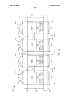
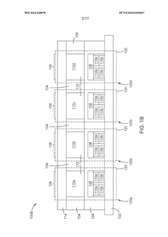
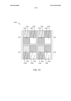
MicroLED displays can incorporate redundant pixel structures to improve yield and allow for pixel repair. This approach involves designing additional sub-pixels or backup LEDs within each pixel, which can be activated if the primary LED fails. The redundant elements can be switched on through various methods, ensuring continued functionality of the display even if individual LEDs become defective.- Redundant pixel structures: MicroLED displays can incorporate redundant pixel structures to improve yield and allow for pixel repair. This approach involves designing additional sub-pixels or backup LEDs within each pixel, which can be activated if the primary LED fails. The redundant elements can be switched on through various methods, including laser cutting or electrical programming, to replace defective pixels and maintain display quality.
- Pixel repair through remapping: Pixel repair can be achieved through remapping techniques, where defective pixels are identified and their functions are reassigned to nearby functional pixels. This method involves sophisticated algorithms and control circuits that can dynamically adjust the display output to compensate for faulty pixels, effectively 'repairing' the image without physical intervention.
- In-situ repair methods: In-situ repair methods for MicroLED displays involve techniques that can fix defective pixels without removing the display from its assembly. These may include laser-based repairs, where precise laser beams are used to correct open or short circuits, or the application of conductive materials to bridge disconnections. Such methods can significantly improve yield rates and reduce manufacturing costs.
- Fault detection and diagnosis systems: Advanced fault detection and diagnosis systems are crucial for effective MicroLED pixel repair. These systems use various sensing technologies and image processing algorithms to identify defective pixels accurately. They can detect issues such as open circuits, short circuits, or brightness variations, enabling targeted repair strategies and improving overall display quality control.
- Modular repair architectures: Modular repair architectures in MicroLED displays allow for easier maintenance and repair of large-scale displays. This approach involves designing the display in smaller, replaceable modules. If a module contains defective pixels, it can be swapped out entirely, reducing downtime and simplifying the repair process. This is particularly beneficial for large public displays or specialized applications where quick repairs are essential.
02 Pixel repair through remapping
Pixel repair in MicroLED displays can be achieved through remapping techniques. This involves redirecting signals from defective pixels to functional neighboring pixels or unused redundant elements. Advanced algorithms and control circuits are used to identify faulty pixels and dynamically adjust the display output, maintaining image quality despite the presence of defects.Expand Specific Solutions03 In-situ repair methods
In-situ repair methods for MicroLED displays involve techniques that can fix defective pixels without removing the display from its assembly. These may include laser-based repair processes, localized heating, or electrical stimulation to reactivate or bypass faulty LEDs. Such methods can significantly improve manufacturing yield and reduce the cost of MicroLED production.Expand Specific Solutions04 Fault detection and diagnosis systems
Advanced fault detection and diagnosis systems are crucial for effective MicroLED pixel repair. These systems use various sensing technologies and image processing algorithms to identify defective pixels, characterize the nature of the faults, and determine the most appropriate repair strategy. Real-time monitoring and adaptive correction techniques can be employed to maintain display quality throughout the device's lifetime.Expand Specific Solutions05 Modular repair architectures
Modular repair architectures in MicroLED displays allow for the replacement of defective pixel groups or display segments. This approach involves designing the display with removable modules or tiles that can be individually replaced if they contain a high number of defective pixels. Such architectures enhance repairability and can extend the lifespan of large-scale MicroLED displays.Expand Specific Solutions
Industry Players
The research on MicroLED pixel repair and redundancy architectures for large-area display backplanes is currently in an emerging stage, with significant market potential as the display industry shifts towards advanced technologies. The market size is expanding rapidly, driven by increasing demand for high-resolution, energy-efficient displays in various sectors. Technologically, the field is still evolving, with companies like VueReal, BOE Technology, and Samsung Display leading innovation. These firms are developing cutting-edge solutions for pixel repair and redundancy, crucial for improving yield and performance in large-area MicroLED displays. Other players like Applied Materials and LG Display are also contributing to the advancement of this technology, indicating a competitive and dynamic landscape.
BOE Technology Group Co., Ltd.
Technical Solution: BOE has developed a proprietary MicroLED pixel repair technology called "Pixel Compensation and Repair" (PCR). This method utilizes redundant sub-pixels and intelligent algorithms to detect and compensate for defective pixels in real-time. The PCR system employs a combination of hardware-based redundancy and software-driven compensation techniques. For large-area display backplanes, BOE implements a modular architecture where each module contains its own repair circuitry, allowing for scalability and improved yield rates. The company has reported achieving defect rates as low as 1 part per million (ppm) for its MicroLED displays using this technology [1][3].
Strengths: High yield rates, scalable architecture, and real-time compensation. Weaknesses: Increased complexity in backplane design and potential power consumption overhead for continuous monitoring and compensation.
Applied Materials, Inc.
Technical Solution: Applied Materials has developed a comprehensive MicroLED repair solution called "Integrated Pixel Repair" (IPR) for large-area display backplanes. Their approach combines in-line inspection, laser repair, and redundancy architectures. The IPR system uses high-resolution optical inspection to identify defective pixels during the manufacturing process. For repairable defects, a precision laser system can remove or reconnect faulty micro-LEDs. In cases where laser repair is not possible, the system activates redundant sub-pixels built into the backplane design. For large-area displays, Applied Materials has created a scalable architecture that divides the backplane into manageable zones, each with its own repair and redundancy systems. This modular approach allows for efficient processing of large panels. The company reports that their IPR technology has improved overall yield rates by up to 40% for MicroLED manufacturing lines [7][9].
Strengths: Combines multiple repair techniques, in-line processing for immediate defect addressing, and scalable zoned architecture. Weaknesses: High initial investment cost and potential for increased manufacturing complexity.
Key Innovations
Repair methods for micro-led displays using intensity averaging
PatentWO2024238878A1
Innovation
- The method involves bonding LEDs to a backplane, inspecting for defective LEDs, and using sub-pixel isolation structures and color conversion materials to create a pixel array where operational sub-pixels can compensate for defective ones by adjusting intensity and color conversion, thereby maintaining display quality.
Redundant pixel architecture in ILED displays
PatentActiveUS20190181060A1
Innovation
- A method is introduced to create sub-pixel assemblies in ILED displays by identifying defective micro-LEDs and replacing them with operable ones, ensuring that each sub-pixel assembly includes either one, two, or three micro-LEDs depending on their status, with a second replacement micro-LED being added if both primary and first replacement micro-LEDs are defective, and physically severing the current path to the defective LEDs to connect the second replacement micro-LED to the current source.
Manufacturing Process
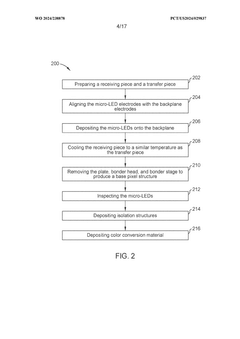
The manufacturing process for MicroLED displays with pixel repair and redundancy architectures involves several critical steps and considerations. The process begins with the fabrication of the MicroLED array on a substrate, typically using epitaxial growth techniques. This is followed by the transfer of individual MicroLEDs to the display backplane, which is a crucial and challenging step due to the microscopic size of the LEDs.
One of the key aspects of the manufacturing process is the implementation of redundancy architectures. This involves designing and fabricating additional MicroLEDs or circuits that can be activated in case of primary pixel failures. The redundancy system may include spare MicroLEDs positioned adjacent to the main pixels or integrated within the pixel structure itself.
The pixel repair process is an integral part of the manufacturing workflow. It typically involves the use of advanced imaging and testing equipment to identify defective pixels. Once identified, these pixels can be repaired or replaced using various techniques. One common method is laser-based repair, where a focused laser beam is used to remove or modify the defective MicroLED. Alternatively, redundant pixels can be activated to compensate for the faulty ones.
Quality control and testing are crucial throughout the manufacturing process. This includes comprehensive electrical and optical testing of individual MicroLEDs, as well as the entire display panel. Advanced inspection systems, often employing machine vision and artificial intelligence, are used to detect defects and ensure uniformity across the large-area display.
The backplane manufacturing process is another critical component. It involves the fabrication of thin-film transistors (TFTs) and other circuitry necessary for driving the MicroLEDs. The integration of repair and redundancy architectures into the backplane design adds complexity to this process, requiring precise alignment and interconnection between the MicroLED array and the underlying circuitry.
Yield management is a significant challenge in MicroLED manufacturing, particularly for large-area displays. The pixel repair and redundancy architectures play a crucial role in improving yield rates. By allowing for the correction of defects and the activation of spare pixels, these technologies can significantly increase the number of usable panels, thereby reducing manufacturing costs and improving overall production efficiency.
Yield Improvement
Yield improvement is a critical aspect of MicroLED display manufacturing, particularly for large-area display backplanes. As the size of displays increases, the probability of defects occurring during the manufacturing process also rises, potentially leading to lower production yields and increased costs. To address this challenge, various strategies have been developed to enhance yield and ensure the quality of MicroLED displays.
One of the primary approaches to yield improvement is the implementation of redundancy architectures. These architectures involve incorporating additional components or circuits into the display backplane to compensate for potential defects. For instance, redundant pixel structures can be integrated into the design, allowing for the activation of backup pixels in case of primary pixel failures. This redundancy significantly reduces the impact of individual defect occurrences on the overall display performance.
Another key strategy for yield improvement is the development of advanced pixel repair techniques. These methods aim to identify and rectify defective pixels during the manufacturing process or even after the display has been assembled. Laser-based repair techniques have shown promising results, enabling the precise removal of defective MicroLEDs and the subsequent replacement with functional ones. This approach not only improves yield but also extends the lifespan of displays by allowing for post-production repairs.
In-line inspection and testing procedures play a crucial role in yield improvement efforts. Advanced imaging and electrical testing systems are employed to detect defects at various stages of the manufacturing process. By identifying issues early on, manufacturers can take corrective actions promptly, reducing the likelihood of defective displays reaching the final stages of production. Machine learning algorithms are increasingly being utilized to enhance the accuracy and efficiency of these inspection processes.
The optimization of MicroLED transfer processes is another area of focus for yield improvement. The transfer of MicroLEDs from the growth substrate to the display backplane is a critical step that can significantly impact yield. Researchers are exploring novel transfer techniques, such as mass transfer methods and selective pick-and-place approaches, to improve the accuracy and reliability of this process. These advancements aim to minimize damage to MicroLEDs during transfer and ensure precise placement on the backplane.
Furthermore, the development of fault-tolerant driving schemes contributes to yield improvement by mitigating the impact of pixel defects on display performance. These schemes involve sophisticated algorithms that can compensate for non-functional pixels by adjusting the brightness and color of surrounding pixels. By implementing such adaptive driving techniques, manufacturers can salvage displays with minor defects that would otherwise be discarded, thereby improving overall production yield.
Unlock deeper insights with Patsnap Eureka Quick Research — get a full tech report to explore trends and direct your research. Try now!
Generate Your Research Report Instantly with AI Agent
Supercharge your innovation with Patsnap Eureka AI Agent Platform!