MicroLED waveguide coupling strategies for compact AR near-eye systems
AUG 21, 20258 MIN READ
Generate Your Research Report Instantly with AI Agent
Patsnap Eureka helps you evaluate technical feasibility & market potential.
MicroLED AR Background
MicroLED technology has emerged as a promising solution for augmented reality (AR) near-eye displays, offering significant advantages over traditional display technologies. This innovative approach combines the benefits of high brightness, low power consumption, and pixel-level control, making it particularly suitable for compact AR systems.
The development of MicroLED displays for AR applications has been driven by the increasing demand for more immersive and realistic visual experiences. As AR technology continues to evolve, the need for compact, lightweight, and high-performance display solutions has become paramount. MicroLED technology addresses these requirements by providing superior image quality, energy efficiency, and form factor advantages.
One of the key challenges in implementing MicroLED displays for AR near-eye systems is the efficient coupling of light from the MicroLED array into the waveguide. This coupling process is critical for achieving optimal image quality and system performance. Various strategies have been explored to address this challenge, including the use of micro-optics, diffractive elements, and advanced waveguide designs.
The integration of MicroLED displays with waveguide technology has opened up new possibilities for creating compact and lightweight AR devices. Waveguides allow for the efficient transmission of light from the display to the user's eye, while maintaining a slim profile. This combination enables the development of AR glasses and headsets that are more comfortable and aesthetically pleasing than their predecessors.
As the field of AR continues to advance, researchers and engineers are focusing on improving the efficiency and performance of MicroLED waveguide coupling strategies. This includes optimizing the design of MicroLED arrays, enhancing the optical properties of waveguides, and developing novel coupling techniques to maximize light extraction and minimize losses.
The potential applications of MicroLED-based AR near-eye systems extend beyond consumer electronics. Industries such as healthcare, manufacturing, and education are exploring the use of this technology for training, visualization, and remote collaboration. The ability to overlay digital information onto the real world with high fidelity and minimal latency opens up new possibilities for enhancing productivity and decision-making in various sectors.
In conclusion, the background of MicroLED waveguide coupling strategies for compact AR near-eye systems represents a convergence of cutting-edge display technology and advanced optical engineering. As research in this field progresses, we can expect to see further improvements in image quality, energy efficiency, and form factor, ultimately leading to more immersive and practical AR experiences across a wide range of applications.
AR Market Analysis
The augmented reality (AR) market has been experiencing significant growth and transformation in recent years, driven by advancements in display technologies, particularly in the realm of compact near-eye systems. The global AR market size was valued at $17.67 billion in 2020 and is projected to reach $97.76 billion by 2028, growing at a CAGR of 24.2% from 2021 to 2028.
The demand for AR technologies is expanding across various sectors, including gaming, entertainment, healthcare, education, and industrial applications. In the consumer segment, AR-enabled smartphones and smart glasses are gaining traction, with major tech companies investing heavily in AR development. The enterprise sector is also adopting AR solutions for training, remote assistance, and workflow optimization, contributing to market growth.
MicroLED technology, coupled with waveguide optics, is emerging as a promising solution for compact AR near-eye displays. This combination offers advantages such as high brightness, low power consumption, and improved form factor, addressing key challenges in AR device development. The market for MicroLED displays in AR applications is expected to grow rapidly, with a projected CAGR of 80.5% from 2021 to 2026.
The AR hardware market, including headsets and smart glasses, is forecasted to reach $36 billion by 2024. This growth is driven by increasing demand for lightweight, high-performance AR devices that can seamlessly integrate into daily life. The development of efficient waveguide coupling strategies for MicroLED displays is crucial in meeting this demand and unlocking the full potential of AR technology.
Key market players in the AR industry, such as Apple, Google, Microsoft, and Facebook, are investing heavily in MicroLED and waveguide technologies. These companies are not only developing hardware but also creating ecosystems and platforms to support AR applications. This trend is expected to accelerate market growth and drive innovation in compact AR near-eye systems.
The Asia-Pacific region is anticipated to witness the highest growth rate in the AR market, with China and Japan leading in technology development and adoption. North America currently holds the largest market share, driven by the presence of major tech companies and a strong focus on research and development.
As the AR market continues to evolve, the demand for more sophisticated and compact display solutions is increasing. The development of efficient MicroLED waveguide coupling strategies for AR near-eye systems is poised to play a crucial role in shaping the future of this market, enabling new applications and improving user experiences across various industries.
Waveguide Coupling Challenges
Waveguide coupling in MicroLED-based AR near-eye systems presents several significant challenges that researchers and engineers must overcome to achieve compact and efficient designs. One of the primary difficulties lies in the inherent divergence of light emitted from MicroLED sources. This divergence makes it challenging to efficiently couple light into the thin waveguide structures typically used in AR glasses, resulting in substantial light loss and reduced overall system efficiency.
Another major hurdle is the need for precise alignment between the MicroLED array and the waveguide input. Even minor misalignments can lead to significant coupling losses and degradation of image quality. This requirement for high-precision positioning adds complexity to the manufacturing process and can impact the scalability of production.
The spectral characteristics of MicroLEDs also pose challenges for waveguide coupling. The broad emission spectrum of typical MicroLEDs can lead to chromatic aberrations and reduced image quality when coupled into waveguides designed for specific wavelengths. This issue is particularly pronounced in full-color displays, where separate coupling strategies may be needed for red, green, and blue MicroLEDs.
Heat management is another critical concern in MicroLED waveguide coupling. The high current densities required for MicroLED operation can generate significant heat, which can affect both the performance of the LEDs and the optical properties of the waveguide. Efficient thermal management strategies must be integrated into the coupling design to ensure stable and reliable operation.
The need for high brightness in AR displays further complicates the coupling challenge. To achieve sufficient brightness for outdoor use, MicroLEDs must be driven at high current densities, which can exacerbate heat generation and potentially reduce the lifespan of the devices. Balancing brightness requirements with power efficiency and device longevity is a key consideration in coupling design.
Miniaturization goals for AR glasses also impose strict size constraints on the coupling interface. Traditional coupling methods, such as bulky lens systems, are often incompatible with the form factor requirements of modern AR devices. This necessitates the development of novel, compact coupling solutions that can maintain high efficiency within a limited spatial envelope.
Lastly, the coupling strategy must be compatible with mass production techniques to be commercially viable. Developing coupling methods that can be reliably implemented in high-volume manufacturing processes, while maintaining the necessary precision and performance, remains a significant challenge in the field of MicroLED-based AR systems.
Current Coupling Solutions
01 Compact MicroLED waveguide structures
Innovative designs for compact MicroLED waveguide structures that minimize overall device size while maintaining optical performance. These structures may incorporate novel materials or geometries to reduce the footprint of the waveguide system.- Compact MicroLED waveguide structures: Innovative designs for compact MicroLED waveguide structures that minimize overall device size while maintaining optical performance. These structures may incorporate novel materials or geometries to reduce the footprint of the waveguide system.
- Integration of MicroLEDs with waveguide components: Techniques for seamlessly integrating MicroLED arrays with waveguide components to create more compact and efficient display systems. This may involve advanced packaging methods or direct bonding of MicroLEDs to waveguide substrates.
- Miniaturized optical coupling systems: Development of miniaturized optical coupling systems to efficiently transfer light from MicroLEDs into waveguides. These systems may use micro-optics, nanostructures, or novel materials to achieve high coupling efficiency in a compact form factor.
- Multilayer waveguide architectures: Design of multilayer waveguide architectures that stack multiple waveguide layers to increase functionality while maintaining a slim profile. This approach can enable more complex optical systems in a compact package.
- Compact driver and control circuitry: Implementation of compact driver and control circuitry for MicroLED waveguide systems. This includes miniaturized electronic components and efficient circuit layouts to reduce the overall size of the display module.
02 Integration of MicroLEDs with waveguide components
Techniques for seamlessly integrating MicroLED arrays with waveguide components to create more compact and efficient display systems. This may involve advanced packaging methods or direct bonding of MicroLEDs to waveguide substrates.Expand Specific Solutions03 Miniaturization of optical coupling elements
Development of miniaturized optical coupling elements to efficiently transfer light from MicroLEDs into waveguides while maintaining a compact form factor. This may include micro-optics, nanostructures, or metamaterials to enhance coupling efficiency.Expand Specific Solutions04 Multilayer waveguide architectures
Design of multilayer waveguide architectures that stack multiple waveguide layers to increase functionality while minimizing lateral expansion. This approach can lead to more compact overall device dimensions for complex display systems.Expand Specific Solutions05 Compact light extraction and beam shaping
Implementation of compact light extraction and beam shaping techniques within the waveguide structure to eliminate the need for bulky external optics. This may involve integrated diffractive or holographic elements to control light output in a space-efficient manner.Expand Specific Solutions
AR Industry Key Players
The MicroLED waveguide coupling for compact AR near-eye systems is in an early growth stage, with a rapidly expanding market driven by increasing demand for AR applications. The global AR market is projected to reach $97.76 billion by 2028, with a CAGR of 48.6%. Technologically, the field is advancing quickly but still faces challenges in miniaturization and efficiency. Key players like Meta Platforms, Google, and Microsoft are investing heavily in R&D, while specialized companies such as Lumus, Dispelix, and DigiLens are developing innovative waveguide solutions. Emerging players from China, including Jiaxing Yuguang and Chengdu Ideal Realm, are also making significant contributions, indicating a competitive and diverse landscape in this cutting-edge technology sector.
Meta Platforms Technologies LLC
Technical Solution: Meta has developed advanced MicroLED waveguide coupling strategies for compact AR near-eye systems. Their approach utilizes a combination of freeform optics and holographic optical elements (HOEs) to achieve efficient light coupling[1]. The system employs a MicroLED display as the light source, which is then coupled into a thin waveguide using a specially designed input coupler. This coupler optimizes the angular distribution of light to maximize coupling efficiency. Within the waveguide, Meta uses a series of strategically placed HOEs to expand the eyebox and control the light propagation[2]. The output coupler is designed to extract light uniformly across the field of view, ensuring a consistent and bright image for the user. Meta's solution also incorporates advanced pupil tracking to dynamically adjust the output coupling, further enhancing the overall visual experience[3].
Strengths: High efficiency light coupling, compact form factor, and dynamic pupil tracking for improved user experience. Weaknesses: Potential complexity in manufacturing HOEs at scale and sensitivity to environmental factors.
Lumus Ltd.
Technical Solution: Lumus has pioneered a unique approach to MicroLED waveguide coupling for AR near-eye displays using their patented Light-Guide Optical Element (LOE) technology[4]. Their system employs a series of partially reflective surfaces embedded within a thin glass waveguide. The MicroLED light source is coupled into the waveguide using a specially designed input coupler that optimizes the incident angle. As light propagates through the waveguide, it undergoes controlled reflections at each partially reflective surface, gradually expanding the eyebox. The final surface acts as an output coupler, projecting the image towards the user's eye. Lumus' technology allows for a wide field of view (up to 50 degrees) while maintaining a slim profile[5]. They have also developed advanced coating techniques to enhance light transmission and reduce unwanted reflections, resulting in improved image quality and brightness[6].
Strengths: Wide field of view, thin profile, and high optical efficiency. Weaknesses: Potential for visible artifacts due to the reflective surface structure and challenges in mass production of complex waveguide elements.
Innovative Coupling Patents
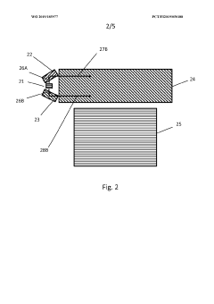
Waveguide element and waveguide stack for display applications
PatentWO2019185977A1
Innovation
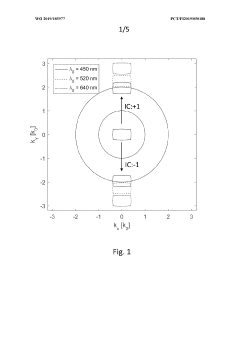
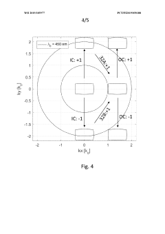
- A waveguide element with an in-coupling grating that splits incoming light into two directions using opposite diffraction orders, with a short period to only couple wavelengths below a threshold in the visible range, and a waveguide stack with separate layers for each color, utilizing reflective and exit pupil expander gratings to optimize surface area and prevent cross-coupling.
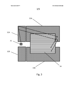
Eyepieces for augmented reality display system
PatentPendingUS20250076658A1
Innovation
- The use of an eyepiece waveguide with an optically transmissive substrate, featuring an input coupling grating (ICG) region, a multi-directional pupil expander (MPE) region, and an exit pupil expander (EPE) region, which collectively couple, expand, and redirect light beams to enhance the field of view and luminance uniformity.
Optical Design Considerations
In the realm of MicroLED waveguide coupling for compact AR near-eye systems, optical design considerations play a crucial role in achieving optimal performance and user experience. The primary challenge lies in efficiently coupling light from MicroLED displays into thin waveguides while maintaining high brightness, wide field of view (FOV), and minimal optical artifacts.
One key aspect of optical design is the selection of appropriate coupling optics. Prism-based couplers offer high efficiency but may increase system bulk, while grating couplers can be more compact but potentially suffer from lower coupling efficiency. Hybrid approaches combining prisms and gratings have shown promise in balancing these trade-offs.
The waveguide design itself is another critical factor. Planar waveguides with surface relief gratings are commonly used, but newer designs incorporating volume holograms or metasurfaces are being explored to enhance coupling efficiency and expand the FOV. The choice of waveguide material, typically glass or plastic, affects both optical performance and manufacturing considerations.
Optimizing the MicroLED array configuration is essential for maximizing light output and minimizing crosstalk between pixels. Factors such as pixel pitch, emitter size, and array layout must be carefully considered in relation to the coupling optics and waveguide design.
Color management presents unique challenges in MicroLED-based systems. Strategies for achieving a wide color gamut while maintaining brightness include optimizing the spectral output of individual LEDs and implementing advanced color filtering techniques within the waveguide structure.
Addressing issues of stray light and ghost images is crucial for image quality. This involves careful design of anti-reflection coatings, light baffles, and absorption layers throughout the optical system. Additionally, techniques for managing polarization states can be employed to enhance contrast and reduce unwanted reflections.
The overall form factor of the near-eye display system must be considered, balancing optical performance with user comfort and aesthetics. This often involves trade-offs between FOV, eye box size, and overall device thickness.
Finally, manufacturability and scalability of the optical design are important considerations. Techniques such as wafer-level optics and roll-to-roll processing are being explored to enable mass production of high-quality, cost-effective AR displays.
Manufacturability Assessment
The manufacturability assessment of MicroLED waveguide coupling strategies for compact AR near-eye systems is a critical aspect that determines the feasibility and scalability of these technologies in mass production. The manufacturing process for MicroLED-based AR systems involves several complex steps, each presenting unique challenges.
One of the primary considerations is the fabrication of MicroLED arrays. The process requires precise control over the epitaxial growth of semiconductor materials, typically using metal-organic chemical vapor deposition (MOCVD) or molecular beam epitaxy (MBE). The uniformity and yield of MicroLED arrays are crucial factors that directly impact the overall system performance and cost-effectiveness.
The integration of MicroLED arrays with waveguide structures presents another set of manufacturing challenges. The alignment between the MicroLED emitters and the waveguide input couplers must be extremely precise, often requiring sub-micron accuracy. This level of precision necessitates advanced pick-and-place technologies and potentially in-situ alignment techniques.
Waveguide fabrication itself is a critical manufacturing step. Various methods such as photolithography, nanoimprint lithography, or direct laser writing can be employed to create the necessary diffractive or holographic structures within the waveguide. The choice of manufacturing method significantly impacts the scalability and cost of production.
The assembly of the entire AR near-eye system requires careful consideration of thermal management, electrical connections, and optical alignment. The compact nature of these systems demands innovative packaging solutions that can withstand the rigors of daily use while maintaining optimal performance.
Quality control and testing procedures are essential throughout the manufacturing process. Advanced inspection techniques, such as automated optical inspection (AOI) and electron microscopy, are necessary to ensure the integrity of MicroLED arrays and waveguide structures. Functional testing of the assembled systems requires specialized equipment to evaluate optical performance, power efficiency, and user experience metrics.
The choice of materials plays a crucial role in manufacturability. Substrate materials for MicroLEDs, waveguide materials, and encapsulants must be selected not only for their optical and mechanical properties but also for their compatibility with high-volume manufacturing processes.
As the industry moves towards larger-scale production, considerations for automation and Industry 4.0 principles become increasingly important. The integration of robotics, machine learning for process optimization, and data analytics for yield improvement will be key factors in achieving cost-effective manufacturing at scale.
Unlock deeper insights with Patsnap Eureka Quick Research — get a full tech report to explore trends and direct your research. Try now!
Generate Your Research Report Instantly with AI Agent
Supercharge your innovation with Patsnap Eureka AI Agent Platform!